


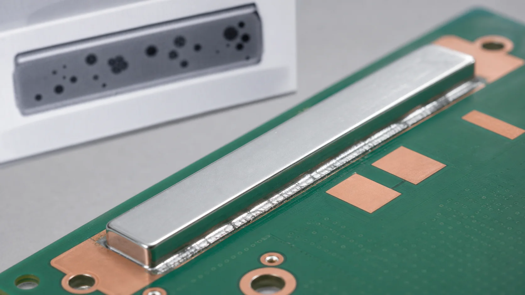
Quick answer: SMD busbar voids, poor wetting and hidden solder separation after reflow cannot be judged only by shiny solder fillets. For high-current PCB hardware, inspect soldered area, edge wetting, void distribution, solder continuity, milliohm voltage drop and real temperature rise together. Before production, review stencil opening, paste volume, reflow profile, X-ray or cross-section sampling and current testing in one process window.
Questions answered on this page
- Why do SMD busbars show voids or poor wetting after reflow?
- How much solder voiding can affect high-current temperature rise?
- How should stencil design, paste volume and busbar thermal mass be reviewed?
- When is X-ray enough, and when is cross-section needed?
- Should production acceptance rely on appearance, voltage drop or temperature rise?
Engineering summary
- Hidden solder separation is difficult to see from the outside on long rectangular SMD busbars.
- Voids often come from poor outgassing, pad contamination, high thermal mass, unsuitable reflow profile or weak flux activity.
- More paste is not always better. Excess paste can create floating, solder beads and large voids.
- High-current reliability depends on solder continuity, effective contact area, local voltage drop and stable temperature rise.
- Production approval should combine visual inspection, X-ray or cross-section, milliohm voltage drop and current temperature-rise testing.
Application context
Engineering issues such as “SMD busbar solder void”, “poor wetting on solderable copper busbar”, “reflow soldering copper bar voids” and “high-current PCB solder joint temperature rise” usually appear during prototype review, pilot production or customer failure analysis. The busbar is both a current path and a large thermal mass; if the soldering process window is wrong, increasing the metal size will not solve the root cause.
Hongchuan Precision Hardware supplies SMD busbars, PCB welding terminals, SMT nuts and copper-aluminum connectors for high-current PCB assemblies.
Separate the problem types first
| Problem | Typical symptom | Check first |
|---|---|---|
| Insufficient solder joint | Local separation and high voltage drop | Pad contamination, plating, reflow heat |
| Poor wetting | Weak edge fillet, dark solder, discontinuity | Surface finish, oxidation, flux activity |
| Voiding | Dark spots or connected cavities on X-ray | Outgassing path, stencil pattern, preheat profile |
| Floating | One end lifted or uneven solder thickness | Paste excess, placement pressure, coplanarity |
| High temperature rise | Hot area near busbar despite acceptable appearance | Effective soldered area, voltage drop, PCB copper exit |
How stencil openings affect voiding
The bottom contact area of an SMD busbar is much larger than a common chip component. During reflow, flux volatiles must escape from the edges. A single large paste opening may look sufficient, but it can trap gas and create large voids. Segmented openings, controlled paste volume and planned outgassing paths usually create a more stable process window.
If busbar thickness is still under review, compare this with SMD busbar thickness selection for high-current PCB. Higher thickness increases thermal mass and makes reflow profile control more important.
Poor wetting depends on finish and storage
Common SMD busbar finishes include tin, nickel, silver and combined plating systems. For reflow soldering, solderability depends on plating thickness, storage time, packaging, oxidation control and surface cleanliness. When wetting is weak, check the PCB pad, busbar finish, paste shelf life and reflow atmosphere together.
For finish selection, see tin, nickel and silver plating selection for SMD busbars.
What X-ray and cross-section can show
| Method | Good for | Limitation |
|---|---|---|
| X-ray | Large bottom voids, connected cavities, uneven solder distribution | Cannot fully prove interface wetting quality |
| Cross-section | Interface wetting, IMC, solder thickness, true void shape | Destructive and limited sample count |
| Visual inspection | Edge fillet, solder beads, shift, floating | Cannot see effective bottom soldered area |
| Milliohm voltage drop | Effective current path and contact stability | Needs stable fixture and repeatable conditions |
| Temperature rise | Real powered thermal risk | Affected by airflow, copper exit and ambient condition |
High temperature rise may not be a busbar-size issue
If the area near the SMD busbar is hot, do not immediately assume the busbar is too small. The real bottleneck may be the PCB copper exit, via array, inner-layer connection or solder mask opening. When temperature-rise data is available, compare it with SMD busbar pad exit overheating troubleshooting.
Validation workflow before production
- Incoming part review. Check finish, packaging, oxidation and contamination of the SMD busbar.
- Stencil comparison. Compare solid, segmented and reduced-paste openings with visual, X-ray and strength data.
- Reflow profile review. Check preheat, ramp rate, peak temperature and time above liquidus, not only the paste datasheet range.
- X-ray or cross-section baseline. Create an early reference for large solder joints and void distribution.
- Voltage drop and temperature-rise retest. Validate with real current, real PCB copper and real assembly conditions.
- Packaging and placement validation. For tape-and-reel supply, check nozzle pickup, orientation and placement offset with SMD copper busbar tape-and-reel packaging requirements.
Common mistakes
- Judging only by edge fillet appearance while ignoring bottom soldered area.
- Using total void percentage as the only criterion without checking void location.
- Reducing paste blindly and losing solder strength or thermal-cycle reliability.
- Changing busbar thickness or plating while keeping the old stencil and reflow profile.
- Replacing the busbar with a larger one without checking PCB copper exit and via array.
RFQ and engineering checklist
- Continuous current, peak current, allowed temperature rise and test environment.
- PCB copper thickness, pad size, solder mask opening and inner-layer connection.
- SMD busbar material, thickness, plating and packaging method.
- Reflow oven capability, nitrogen or air atmosphere, solder paste type and stencil thickness.
- X-ray, cross-section, voltage drop, temperature rise and thermal-cycle acceptance criteria.
FAQ
Does any void mean the SMD busbar is unacceptable?
No. Review void percentage, location, continuity, whether the void is in the main current path, and whether voltage drop and temperature rise remain stable.
Can thicker copper solve hidden solder separation?
Usually not. Hidden separation is an interface and process-window issue. A thicker busbar may increase thermal mass and make reflow harder.
When is cross-section required?
Use cross-section when X-ray shows abnormal voids, voltage drop or temperature rise is unstable, or the customer requires proof of interface wetting.
What can Hongchuan support?
Hongchuan can support SMD busbar samples, dimensional review, finish selection, tape-and-reel orientation and drawing confirmation. Start with the high-current PCB hardware selection guide for early selection.