


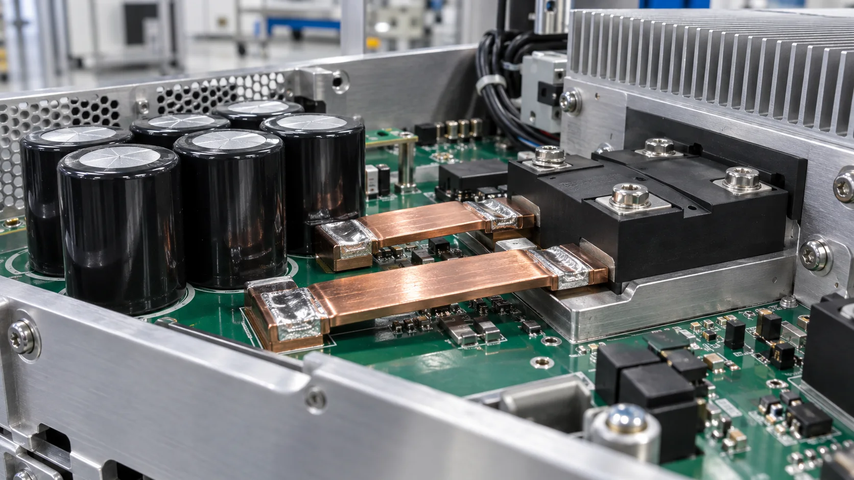
Quick answer: Select an SMD busbar for semiconductor equipment by creating a short, low-resistance and repeatable path between DC link, capacitors and power modules. Review pad exits, vias, reflow heat, parasitics, cooling, vibration and service loads instead of adding copper thickness alone.
Questions answered on this page
- Why use SMD busbars on semiconductor equipment power boards?
- How should the DC-link to module path be optimized?
- How should thick-bar pads and reflow be validated?
- How can maintenance and vibration affect joints?
- How should production controls be built?
Application context
Wafer, packaging and inspection tools often connect rectifiers, DC-link capacitors, IGBT or SiC modules, filters and terminals in limited space. SMD busbars shorten high-current paths and reduce drop and high-frequency loop area. Hongchuan supplies SMD busbars matched to current, ripple, switching, stack-up, copper, pads, heat and assembly.
Trace the real path
| Area | Review | Risk |
|---|---|---|
| DC link | Capacitor exit, ripple loop and pad | Drop and parasitics |
| Busbar body | Section, length, bend and spacing | Rise or insulation loss |
| PCB exit | Copper transition, vias and inner receiving area | Exit hot spot |
| Module end | Terminal, cooling and tolerance | Current concentration |
Trace top, inner layers, vias and device terminals from both bar ends. See SMD busbar pad-exit troubleshooting.
Reflow, temperature and service
Thick copper absorbs heat and can create different wetting, coverage or placement at both pads. Validate stencil, paste, flatness, board support and profile with the real bar. After reflow inspect coverage, voids, offset and lift with X-ray or cross-section. Under rated, ripple and switching loads, measure body, exits, vias, modules and nearby devices, then repeat drop and joint checks after service and vibration. See SMD busbar reflow inspection.
FAQ
Is shorter always better?
Short paths usually help drop and parasitics, but pads, heat spreading, spacing, assembly and service clearance still govern.
Does normal solder appearance prove release?
No. Check internal coverage, voids, segmented drop and powered temperature.
How should samples be specified?
Provide current, ripple, switching, board, copper, pads and reflow conditions. Use the high-current PCB hardware selection guide.