


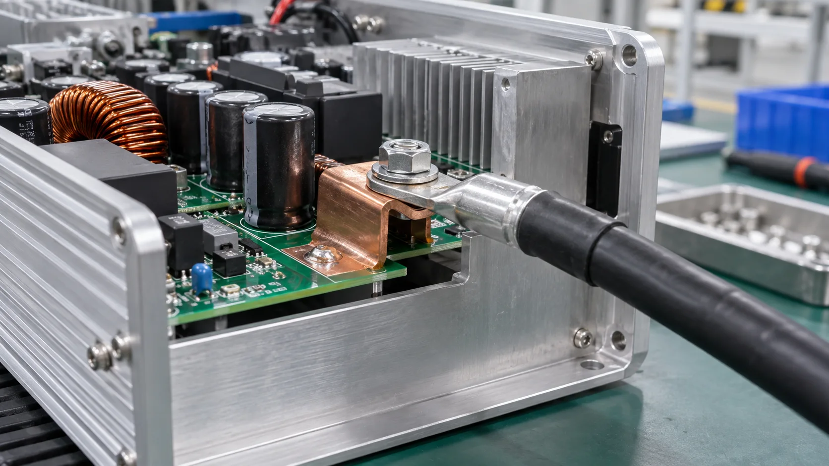
Quick answer: A microinverter AC output terminal must address continuous and overload current, cable-lug contact, phase spacing, enclosure sealing and outdoor thermal cycling. Hole and pad set the solder window, the lug and bolt set interface resistance, and the strain relief keeps cable bending out of the PCB joint. Validate stable temperature, spacing, tolerances, cycling and post-vibration resistance.
Questions answered on this page
- Which parameters matter for a microinverter AC terminal?
- How should hole, pad and lug be matched?
- How should line, neutral and PE spacing be maintained?
- How do outdoor cycling and condensation affect resistance?
- How can prototype checks become production controls?
Application context
A microinverter converts module DC to grid AC, with the AC output between the inverter PCB and external cable. The path can include bridge or filter, PCB copper or SMD busbar, terminal leg, hole solder, terminal body, lug and cable. Hongchuan supplies PCB welding terminals and SMD busbars.
Four selection boundaries
| Boundary | Review | Risk |
|---|---|---|
| Electrical | Continuous, peak, drop and rise | Local heating |
| Insulation | Line, neutral, PE and housing | Spacing loss after tolerances |
| Mechanical | Lug, bolt, strain relief and board support | Fatigue and bend |
| Environment | Temperature, condensation and humidity | Oxide and drift |
Match hole, pad and lug
The hole must satisfy lug and bolt, overlap, insertion tolerance and solder fill. A small hole damages plating or blocks assembly; an oversized hole reduces solder and annulus. Use a gradual pad exit into adequate inner copper and a strain relief for cable weight. See PCB terminal hole and pad design.
Spacing and outdoor validation
Terminal edges, bolt heads, lugs, solder peaks, housing ribs and seals can define the real AC boundary. Review PCB, terminal, bolt, enclosure and assembly tolerances together for line-neutral, line-PE and live-to-housing spacing. Large pads or copper bars may reduce spacing even as they improve temperature.
Run rated and real AC waveform loads through thermal cycling, condensation or humidity and vibration. Measure terminal body, solder, copper exit, lug face and enclosure temperature. Repeat segmented drop, contact resistance and insulation checks after exposure. See SMD busbar pad-exit troubleshooting.
Production release
| Area | Inspection | Record |
|---|---|---|
| Incoming | Dimensions, finish and appearance | Lot result |
| Solder | Fill, wetting and offset | Process and sampling |
| Assembly | Lug, torque and strain relief | Tool and torque |
| System | Rise, spacing and sealing | Load and environment |
FAQ
Is continuous current enough?
No. Check overload, spacing, cable load, temperature swing and contact resistance.
What if resistance rises after cycling?
Measure body, solder, copper exit and lug interface separately, then inspect torque retention, finish, condensation and support.
How should samples be requested?
Provide current, cable size, hole, board, copper, bolt and enclosure space. Use the high-current PCB hardware selection guide.