


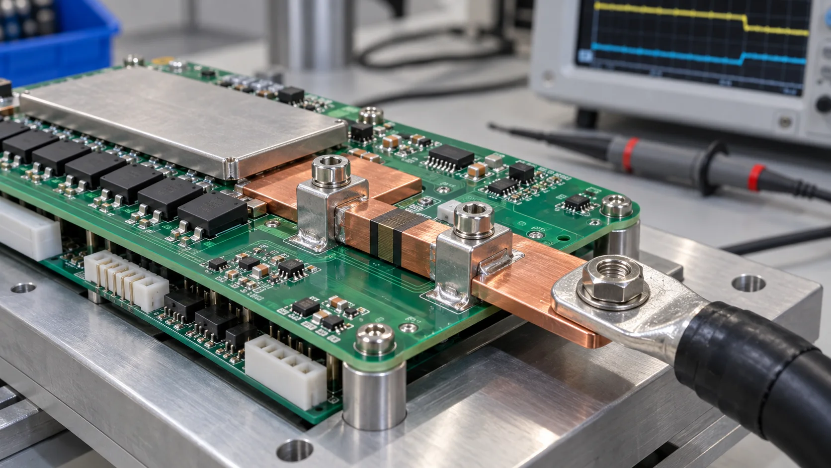
Quick answer: Select a BMS shunt terminal for the complete electrical path, not only main current. Separate the high-current path from the millivolt Kelvin-sense path. The sense points should stay on the defined shunt element so terminal, solder and copper drops are not included in the measurement. Validate current, sense voltage, joint temperature and post-cycle drift together.
Questions answered on this page
- Why does a BMS shunt need a dedicated sampling terminal?
- How should main current and millivolt sensing be separated?
- How do solder and PCB copper affect sensing?
- What should be rechecked after heat, cycling and vibration?
- How can the design become a production inspection plan?
Application context
A battery-management system measures pack charge and discharge current through a shunt. The shunt produces a millivolt differential signal for an amplifier or AFE. A PCB welding terminal connects the busbar, lug or pack cable, while sense copper is routed from defined points on both sides of the shunt. Hongchuan supplies PCB welding terminals, SMD busbars and copper-aluminum hardware.
Separate the two paths
| Path | Function | Focus |
|---|---|---|
| Main | Pack current | Section, contact resistance and rise |
| Kelvin sense | Shunt millivolt signal | Point location, symmetry and isolation |
| Mechanical | Cable and assembly load | Support, torque and board bending |
Route sense traces from the defined shunt ends and keep terminal pads, vias and switching nodes out of the sense loop. Use forward and reverse current to check asymmetry.
Do terminal joints affect millivolt sensing?
They can. Terminal legs, hole solder, pads and copper exits have current-dependent drop. If the sense points include these areas, the measured voltage contains connection drop. Define both Kelvin points on the drawing, provide adequate main-path copper, keep sense traces away from high di/dt nodes and use four-wire measurements to separate shunt, terminal, solder and copper.
When a terminal body is cool but a pad exit is hot, see PCB terminal temperature and contact-resistance testing instead of correcting the error only in software.
Temperature and drift validation
At low, rated, peak and reverse current, record shunt voltage, terminal temperature, solder temperature, copper-exit temperature and ambient. Calculate resistance after thermal stability. Repeat after thermal cycling, vibration and cable-load testing. Check millivolt repeatability, zero drift, joint condition and support deformation.
Production inspection
Production may use sampling for long current runs, but dimensional and electrical controls should be linked. Inspect terminal hole, leg height, pad offset, hole fill, shunt sense points, sense voltage and main-path resistance. Use thermal imaging, cross-section or X-ray for critical lots and retain current, process and lot records.
FAQ
Can the sense trace connect directly to the terminal pad?
Only after the error is defined and validated. A BMS shunt normally benefits from Kelvin points on the shunt element itself.
Does terminal temperature automatically cause sensing error?
It can change resistance and drop, but impact depends on sense-point location. Measure sense voltage and segmented terminal drop together.
What inputs are needed for samples?
Provide main current, shunt resistance, sense points, board, copper and solder process. Use the high-current PCB hardware selection guide.