


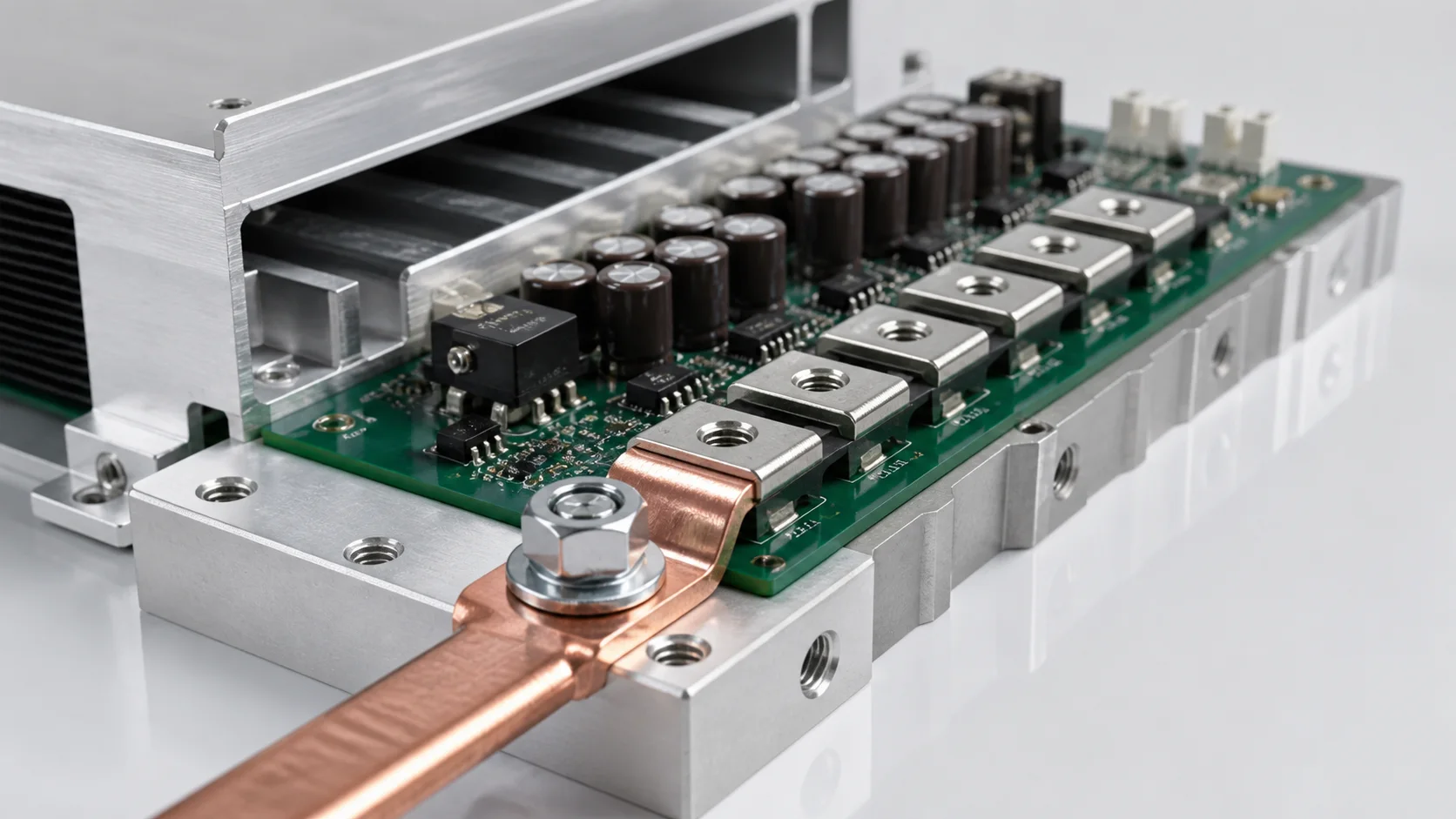
Quick answer: Design a DC fast-charging module output terminal as one complete path: module bus, PCB solder joint, terminal interface, lug and external bus. For parallel modules, use matched paths and segmented drop to verify sharing, then validate temperature at the terminal, joint, lug and bolt interface. A terminal current rating alone does not prove that every parallel branch is reliable.
Questions answered on this page
- Why can a fast-charging output terminal develop a local hot spot?
- How can parallel branches share current more evenly?
- How should lug, bolt and contact surfaces be controlled?
- How should PCB solder and external bus support be combined?
- What should be checked from prototype to production?
Application context
Power modules in fast-charging cabinets often connect in parallel to a DC output bus. Capacitors, switches and output copper feed a PCB welding terminal, then a lug, bolt or short bar connects to the cabinet bus. Hongchuan supplies PCB welding terminals, SMD busbars and copper-aluminum hardware.
Current sharing starts with path impedance
| Area | Risk | Validation |
|---|---|---|
| Module to terminal | Different copper length or layers | Branch drop |
| Terminal and lug | Contact, torque or finish variation | Four-wire resistance |
| Module to bus | Different cable length or bend | Branch current |
| Bus junction | Asymmetric layout | Thermal scan |
Match branch length, section, layer and contact area where possible. Measure rated, peak and ripple conditions. If geometry cannot be symmetric, keep a design margin for balancing and re-test.
Lug, bolt and terminal interface
Real conductive area depends on flatness, burrs, finish and clamp force. Select the terminal hole for the lug and bolt together, including edge width, tool access and HV spacing. Use a controlled torque window and support cable weight and bending through the enclosure or bracket. See PCB terminal temperature and contact-resistance testing.
Welding and board design
Review hole, pad, inner copper and copper exit together. A narrow pad exit can heat the PCB even when the terminal body is cool. Selective solder, wave solder or local rework must be verified with hole wetting, X-ray or cross-section. For short high-current PCB paths, see SMD busbars and SMD busbar reflow inspection.
Validation checklist
| Stage | Work | Evidence |
|---|---|---|
| Design | Path, hole, spacing, support and symmetry | Point map and tolerances |
| Prototype | Branch current, drop and stable rise | Rated and peak data |
| Reliability | Thermal, vibration, overload and torque retention | Drift |
| Production | Solder, torque, appearance and sampling | Control plan |
FAQ
Should the terminal be replaced first when sharing is uneven?
Measure branch current and segmented drop first. Cable length, copper path, bus junction and contact interface can all be responsible.
Where should temperature be measured?
Measure the terminal body, solder or leg, pad exit, lug face, external bus and nearby power devices, with ambient and stable duration.
How can samples be specified?
Provide current, board, copper, hole, lug, bolt and solder process. Use the high-current PCB hardware selection guide.