


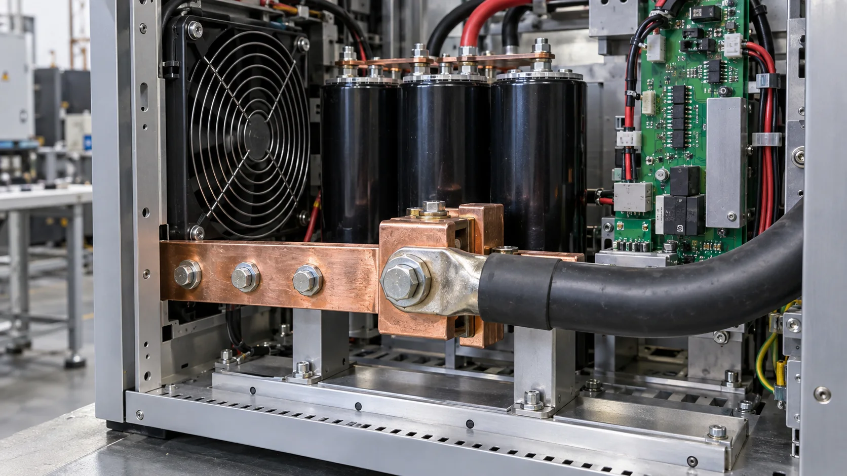
Quick answer: Select a PCB welding terminal for a vacuum-coating power supply by checking pulse current, duty time, pad exit, bar or cable support, cabinet airflow, live-part spacing and post-reflow quality, not current rating alone.
Questions answered on this page
- Why use PCB welding terminals in coating power supplies?
- How do pulse current and long operation affect temperature?
- How should pads, copper and vias form a low-resistance path?
- How should high-voltage clearance include assembly tolerance?
- What belongs in production sampling?
Application context
Vacuum-coating equipment transfers pulsed or continuous power between supplies, filter capacitors, switches, matching networks and chamber interfaces. A PCB welding terminal connects a bar, heavy cable and power board while facing high voltage, heat accumulation and service loads. Hongchuan supplies PCB welding terminals matched to voltage, waveform, pulse, cable, board, copper, direction, airflow and insulation.
Four design boundaries
| Boundary | Review | Risk |
|---|---|---|
| Current | Continuous, peak, pulse, frequency and drop | Terminal or pad hot spot |
| Thermal | Run time, airflow, heat sources and cabinet temperature | Heat accumulation |
| Insulation | Burrs, solder protrusion, housing and spacing | Leakage or creepage |
| Manufacturing | Pad, stencil, reflow, inspection and rework | Void, offset or poor wetting |
Temperature under pulse current
Cover working pulses, stable coating, repeated starts and longest run. Measure terminal, solder leg, pad exit, vias, bar joint and nearby insulation, and use four-wire drop. If the pad exit is hotter than the terminal, inspect copper neck-down, inner receiving layers and vias. See high-current pad-exit troubleshooting.
High-voltage insulation and reflow
The live boundary includes terminal, solder protrusion, bar ends, device terminals, heat sink and metal chamber. Add board thickness, placement offset, burrs and housing tolerance when checking clearance and creepage. Large terminals change reflow heat; inspect wetting, coverage, voids, verticality and board support, using X-ray inspection when needed. Establish resistance, drop, temperature and insulation baselines, then repeat after thermal, vibration and service exposure.
FAQ
Can average current size the terminal?
No. Peak, repetition, pad exit and cooling change the actual load.
Is sufficient spacing alone enough for high voltage?
No. Include solder, burrs, offset, contamination and post-service condition.
How should samples be specified?
Provide waveform, pulse, cable, board, copper, airflow and insulation. Start with the welding terminal product page.