


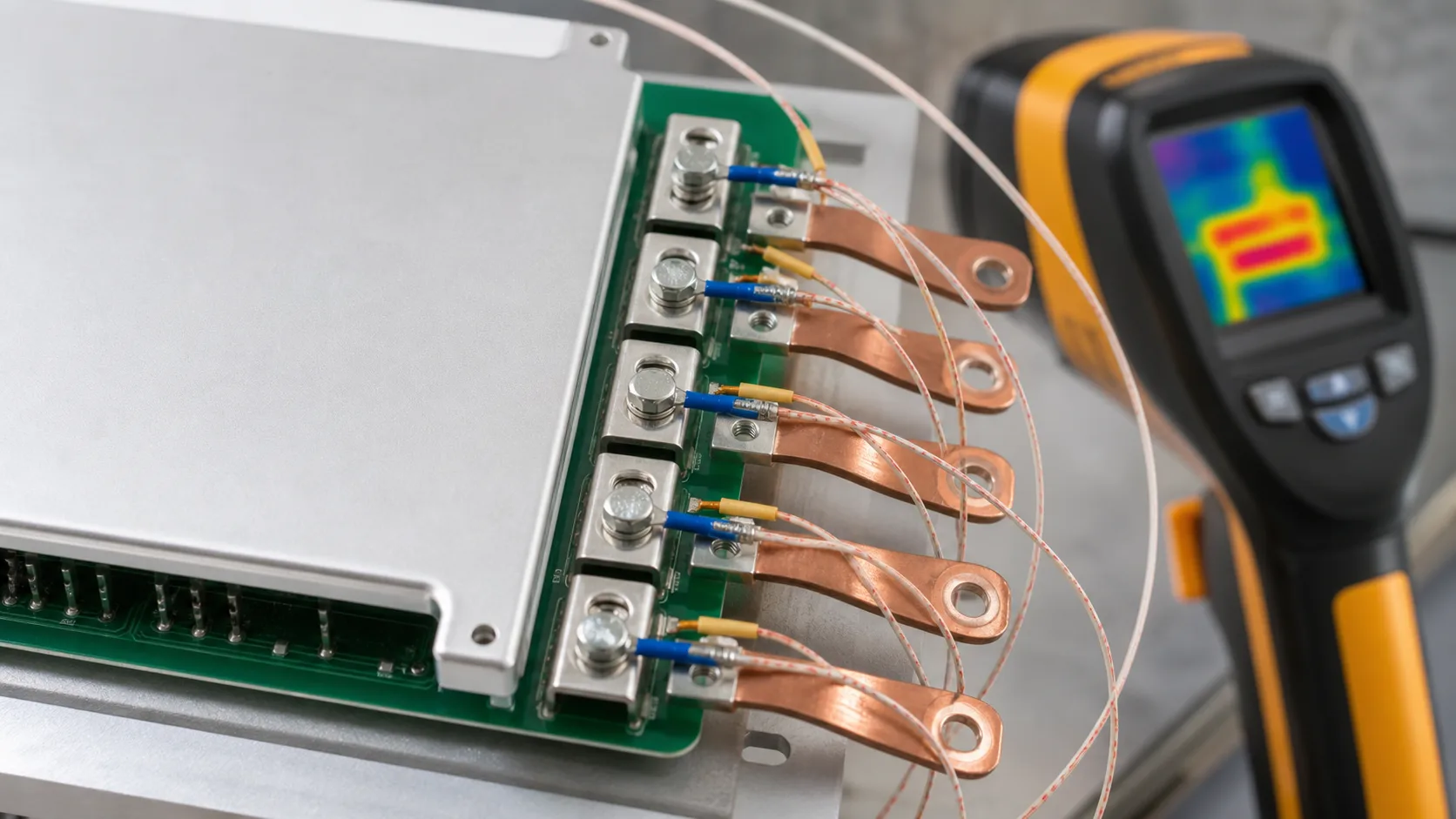
Quick answer: PCB welding terminal temperature-rise testing should record current, ambient, terminal-body temperature, solder temperature, PCB copper-exit temperature and segmented drop. A cool terminal body does not prove a reliable joint or copper path. Fix the test boundary first, separate the resistance of the terminal, solder, PCB and external contact with four-wire measurements, and then judge the result with stable duration, overload, thermal cycling and vibration data.
Questions answered on this page
- Which points should be measured?
- How should current, ambient and stable duration be set?
- How can terminal, solder and PCB problems be separated?
- How should contact resistance correlate with rise and drop?
- How can prototype data become production criteria?
Application context
PCB welding terminals are used in charging-module outputs, OBC battery sides, energy-storage clusters, UPS, inverters and industrial power supplies. The path can include terminal legs, hole solder, pads, copper, bolts and cable-lug contact. Hongchuan supplies PCB welding terminals, SMD busbars, SMT nuts and copper-aluminum hardware.
Fix the test boundary first
Record rated, peak, ripple and overload current, duration, ambient, airflow, enclosure, cooling, board thickness, copper, hole, pad, solder method, lug, bolt, washer, torque and cable position. Also record instrument calibration and probe locations.
Temperature points
| Point | Question | Comparison |
|---|---|---|
| Terminal center | Does section match cooling? | Ambient and equivalent part |
| Leg and solder | Is the joint abnormal? | Both joints, X-ray or cross section |
| Pad/copper exit | Is there a board bottleneck? | Exit-to-joint difference |
| Lug/busbar face | Is the bolted interface resistive? | Segmented drop |
| Enclosure and devices | Is there thermal coupling? | Ambient and airflow baseline |
Why segmented drop matters
Temperature shows where the heat is; it does not prove where the resistance is. Divide the path into terminal body, leg/solder, pad exit, PCB copper, bolted contact and external bar. High drop plus high temperature points to a local resistance bottleneck. High temperature with low drop suggests thermal coupling. Post-cycle drop increase suggests cracking, loosening, finish wear or pressure loss. See PCB terminal temperature and contact-resistance testing.
Stable duration and acceptance
Terminal, PCB copper and heat sinks have different thermal time constants. Record start time, temperature, drop and the time to stability. Use temperature rise, absolute temperature, segmented drop and adjacent-device temperature together. Limits must follow the project material, insulation and system requirements.
Validation matrix
| Stage | Validation | Output |
|---|---|---|
| Design | Path, hole, pad, copper and support | Point map and criteria |
| Prototype | Solder, drop, rise and torque | Hot spots and actions |
| Reliability | Thermal, vibration, humidity and overload | Drift and joint state |
| Pilot | Sampling, tool capability and traceability | Control plan |
FAQ
What temperature rise is acceptable?
No universal value applies without ambient, material, insulation, adjacent devices and system limits. Use rise, absolute temperature, drop and post-cycle drift.
Is a hot solder joint serious if the terminal is cool?
It can be. Check hole fill, wetting, pad exit and joint cross section because the joint or leg may be the hidden resistance bottleneck.
Can Hongchuan support testing?
Yes. Confirm current, board, copper, hole and solder process for samples and key dimensions. Start with the high-current PCB hardware selection guide.