


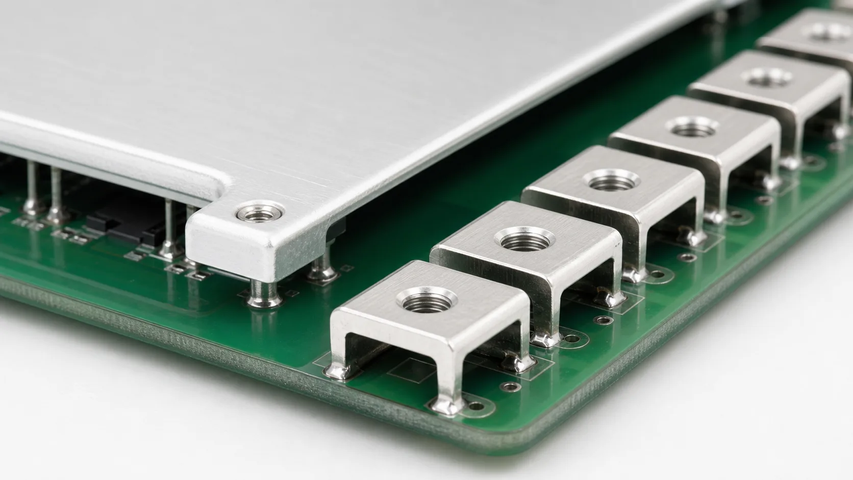
Quick answer: Hole and pad design for a high-current PCB welding terminal should not be based only on whether the terminal leg can fit into the hole. A tight hole can cause insertion damage and poor solder fill. An oversized hole can reduce positioning stability and leave voids inside the joint. The safer approach is to review terminal leg tolerance, finished hole size, copper thickness, soldering process, pull-force requirement and temperature rise together.
Questions answered on this page
- How should the PCB hole size be selected for a welding terminal?
- Why does pad geometry affect temperature rise in a high-current terminal?
- How are solder fill, pull force and electrical resistance connected?
- What changes between wave soldering, selective soldering and manual soldering?
- What should be checked before production release?
Engineering summary
- Start from the maximum material condition of the terminal leg, then include PCB drilling, plating and finished-hole tolerance.
- The pad must support both solder inspection and current spreading into the copper area.
- Poor solder fill is often caused by heat balance, hole clearance, plating or flux activity, not only by insufficient solder amount.
- Pull-force test and temperature-rise test should be treated as two different validations.
Application context
Engineering issues such as “PCB welding terminal hole size”, “high current terminal pad design” and “solder fill problem on PCB terminal” usually appear when engineers are already working on a prototype or production issue. The problem is practical: difficult insertion, poor wetting, terminal tilt, insufficient pull force, blackened pads or local temperature rise.
Hongchuan Precision Hardware focuses on PCB welding terminals, SMD busbars, SMT nuts and other high-current PCB hardware. This article connects hole size, pad design, soldering and validation so hardware, process and sourcing teams can review the same checklist.
Three dimensions to confirm first
| Dimension | What to check | Risk if missed |
|---|---|---|
| Terminal leg | Width, thickness, corner radius, burr and plating thickness | Insertion jam, plating damage, terminal tilt |
| Finished PCB hole | Drill, plating, finished hole tolerance and barrel copper | Too tight or too loose soldering window |
| Process clearance | Solder flow space for wave, selective or manual soldering | Low solder fill, voids, weak joint |
Pad size supports both soldering and heat spreading
A welding terminal is not only a mechanical part. In a high-current PCB, the solder joint is also the transition point where current enters the PCB copper. If the pad is too small, the soldered area becomes weak and the current path narrows sharply at the pad exit.
A practical design keeps a visible solder inspection area around the terminal leg and connects the pad to a wide copper area, copper pour or SMD busbar reinforcement. This reduces local current density and makes inspection easier.
Do not solve poor solder fill only by adding solder
| Symptom | Check first | Action |
|---|---|---|
| Solder at opening but low fill inside | Preheat, hole clearance, barrel heat capacity | Review thermal profile and finished hole size |
| One side wets better than the other | Terminal centering and pad thermal balance | Check insertion verticality and copper connection |
| Dull or non-wetting solder joint | Plating, oxidation, flux activity | Review tin, nickel or silver plating choice |
| Pull force passes but temperature is high | Effective conductive area and pad exit bottleneck | Widen copper or add conductive reinforcement |
Validation before production
- First article dimensional check. Measure terminal leg, finished hole, pad geometry and insertion verticality.
- Solder cross-section. Confirm barrel fill, wetting and voids when the risk is high.
- Pull or push test. Validate mechanical strength under assembly and harness load.
- Powered temperature-rise test. Measure terminal body, solder joint, pad exit and adjacent copper area.
- Process-window review. Recheck the design after PCB thickness, copper weight, plating or soldering process changes.
FAQ
Is a larger hole always better for soldering?
No. An oversized hole may reduce positioning stability and leave insufficient fill. Hole size must balance insertion, solder flow and mechanical location.
Does a larger pad always reduce temperature rise?
No. The current path from the terminal into the copper must be continuous and wide enough. An isolated large pad has limited benefit.
Does plating affect soldering?
Yes. Plating thickness affects actual part size, while plating type affects wetting, resistance and corrosion resistance.
What can Hongchuan provide?
Hongchuan can support terminal dimensions, material and plating suggestions, sample review and high-current PCB hardware selection. The selection guide is a useful starting point for combining welding terminals, SMD busbars and SMT nuts.