


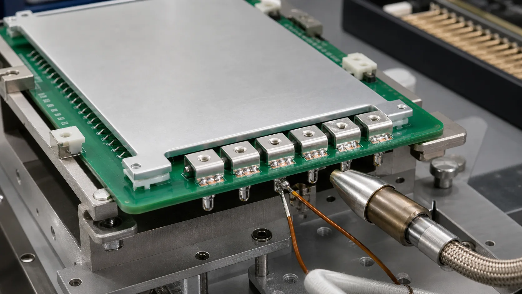
Quick answer: Selective or wave soldering for a PCB welding terminal depends on thermal mass, part count, component shadowing, solder flow, hole fill, flux and takt time. Selective soldering suits local high-mass terminals near sensitive components; wave soldering suits stable volume but needs board direction, masking and flow control. Neither process can be accepted from the external fillet alone. Verify hole fill, wetting, cross sections or X-ray, temperature rise and mechanical performance.
Questions answered on this page
- Which terminals suit selective or wave soldering?
- How should preheat and dwell change with thermal mass?
- Why can a full fillet still hide poor hole fill?
- How do flux, masking and board direction affect soldering?
- How can production inspection be defined?
Application context
PCB welding terminals connect cables or busbars in charging modules, OBCs, energy-storage PCS, UPS, inverters, power supplies and industrial controllers. Hongchuan supplies PCB welding terminals; legs, holes, pads and external fastening must be reviewed with the process equipment.
Selective versus wave boundary
| Factor | Selective | Wave |
|---|---|---|
| Best fit | Local terminals near sensitive parts | Many through-hole parts and volume |
| Controls | Nozzle, preheat, dwell and position | Board direction, wave height, speed and mask |
| Risks | Insufficient heat or access | Shadowing, bridging and thermal shock |
| Inspection | Hole fill, wetting and local heat | Coverage, bridges and hole fill |
Thermal mass and preheat
Large-current terminals absorb more heat. Place thermocouples near legs, pads and sensitive components. Verify flux coverage, preheat slope, nozzle access, solder temperature, dwell and conveyor speed as a process window rather than a single machine setting.
Why hole fill matters
The high-current path includes barrel, leg and hole solder. A good outer fillet can coexist with non-wetting, voids or insufficient fill inside the hole. Hole, annulus and mask design can be reviewed in PCB welding terminal hole and pad design. For high-current or mechanically loaded terminals, add X-ray, cross sections, pull, torque and powered drop/rise checks.
Cleaning, rework and production
Flux residue can affect HV insulation, corrosion and long-term resistance. Define cleaner, time, drying, ionic or visual checks, rework count and post-rework resistance. Use first-article process confirmation, hole-fill inspection, electrical sampling and mechanical checks. See flux-residue and corrosion troubleshooting.
FAQ
Is selective soldering always more reliable?
No. It controls local heat well, while wave suits volume. Reliability depends on the actual window, fill and validation.
Does poor hole fill affect high current?
Yes. Hole solder contributes to conduction and mechanical support, so poor fill can increase drop, rise and cycling risk.
Can Hongchuan support process review?
Yes. Match leg, hole, board, copper, equipment and interface requirements. Start with the high-current PCB hardware selection guide.