


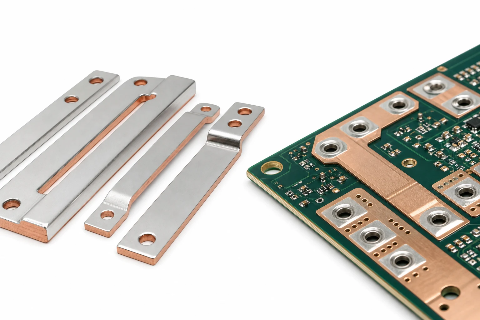
Quick answer: Thick-copper PCB traces spread current through the board, while solderable copper busbars reinforce local high-current bottlenecks. In BMS power boards, the best solution is often a combination.
Questions answered on this page
- Can an SMD copper bar replace a thick-copper PCB?
- When should BMS boards use local solderable busbars?
- Where does the cost difference come from?
Engineering summary
- Use thick copper for board-level current distribution and solderable busbars for local bottleneck reinforcement.
- The most robust design is often a combined solution, not a simple replacement.
Different jobs
Thick copper PCBs are useful for broad power planes and simple assembly. Solderable copper busbars are better when the hot spot is local: a terminal exit, via array, fuse area or MOSFET current-sharing point. See SMD busbars and the selection guide.
Comparison
| Item | Thick copper PCB | Solderable busbar |
|---|---|---|
| Best use | Wide current plane | Local reinforcement |
| Cost | Whole PCB | Metal part and assembly |
| Risk | PCB fabrication limits | Soldering window |
Checklist
- Locate the hot spot first.
- Confirm PCB copper thickness and line width.
- Check reflow capability for the busbar.
- Measure temperature at both ends of the busbar.
FAQ
Can busbars replace thick copper?
They can reduce local bottlenecks, but they do not replace all board-level copper planning.