


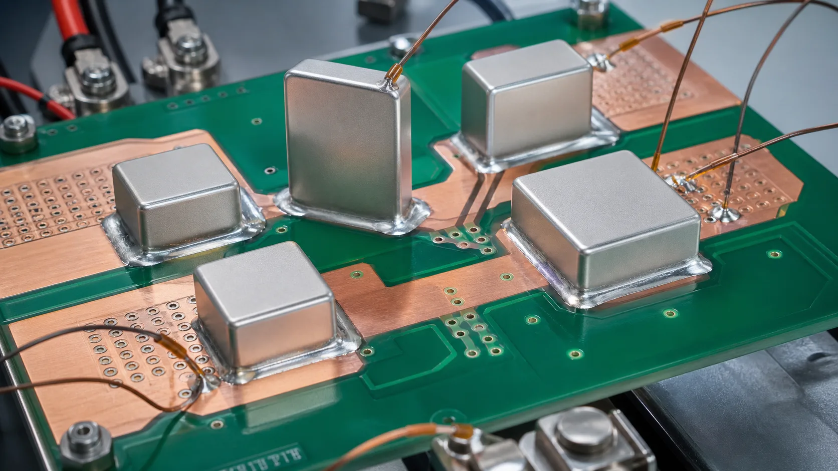
Quick answer: When an SMD busbar body is cool but its pad exit is hot, first check whether current narrows abruptly as it enters the PCB. Review pad-exit width, copper neck-down, layer-change vias, inner-layer receiving copper, slot edges and parallel paths. Use segmented drop and temperature to locate the bottleneck before widening the exit, adding vias, changing the stack-up, changing the pad or changing bar count. Increasing busbar thickness alone usually does not solve a PCB-interface bottleneck.
Questions answered on this page
- Why does the pad exit heat before the bar body?
- How should exits and via arrays be reviewed?
- How should parallel sharing be checked?
- How can segmented drop locate the hot spot?
- How do reflow and production avoid interface defects?
Application context
SMD busbars are used in OBCs, energy-storage PCS, solar inverters, UPS, servo drives and high-power supplies between capacitors, power modules, rectifiers and terminals. Hongchuan supplies SMD busbars and related high-current PCB hardware.
Trace the current path
The path is usually busbar body, two solder joints, SMD pads, copper exits, via array or inner copper, and device or capacitor terminal. Every transition can create a current-density peak. A stable body section does not mean the pad and PCB can receive the same section.
| Area | Check | Typical issue |
|---|---|---|
| Pad exit | Width, corner and transition | Sudden neck-down |
| Via array | Diameter, count, plating and distribution | Layer bottleneck or imbalance |
| Inner receiving area | Copper, stack-up and return path | Congestion and concentration |
| Slot edge | Edge distance and copper continuity | Reduced effective width |
Layout review
- Trace both ends to the next power node, including inner layers.
- Mark the narrowest necks, transitions and via clusters.
- Use gradual transitions instead of wide metal into narrow copper.
- Match length, layer, width, pads and vias for parallel branches.
- Recheck HV spacing, nearby heat sources and heat-sink clearance.
See SMD busbar thickness selection, then validate the PCB receiving area.
Segmented drop and temperature
At the same current, ambient and stable duration, measure body, joints, pad exit, vias and next copper. Thermal imaging finds heat; four-wire drop finds resistance. High exit drop points to copper, pad or layer receiving. One abnormal joint points to paste, wetting, voids or placement. Different parallel drops point to path or pad asymmetry. See pad-exit and via-array troubleshooting.
Parallel sharing and reflow
Parallel bars should use matched length, layer, width, pads and vias. Solder voids, paste height and thermal boundaries also change branch impedance. High thermal mass requires dedicated stencil, paste, support and profile validation with thermocouples at the bar center, pads and nearby devices. Use X-ray for coverage and voids; see SMD busbar reflow defect troubleshooting.
Validation matrix
| Stage | Validation | Output |
|---|---|---|
| Layout | Exits, vias, inner copper and branches | Points and redesign |
| Prototype | Placement, reflow, X-ray, drop and rise | Window and hot spots |
| Reliability | Overload, thermal and vibration | Drift and joint state |
| Pilot | Stencil, placement and sampling | Control plan |
FAQ
Will more busbar thickness fix pad-exit heating?
Usually not. If copper, vias or inner receiving area are the bottleneck, the heat remains at the interface.
Are more vias always better?
No. Diameter, plating, distribution, inner copper and current path must match.
Can Hongchuan support selection?
Yes. Confirm current, board, copper, pads and reflow for samples. Start with the high-current PCB hardware selection guide.