


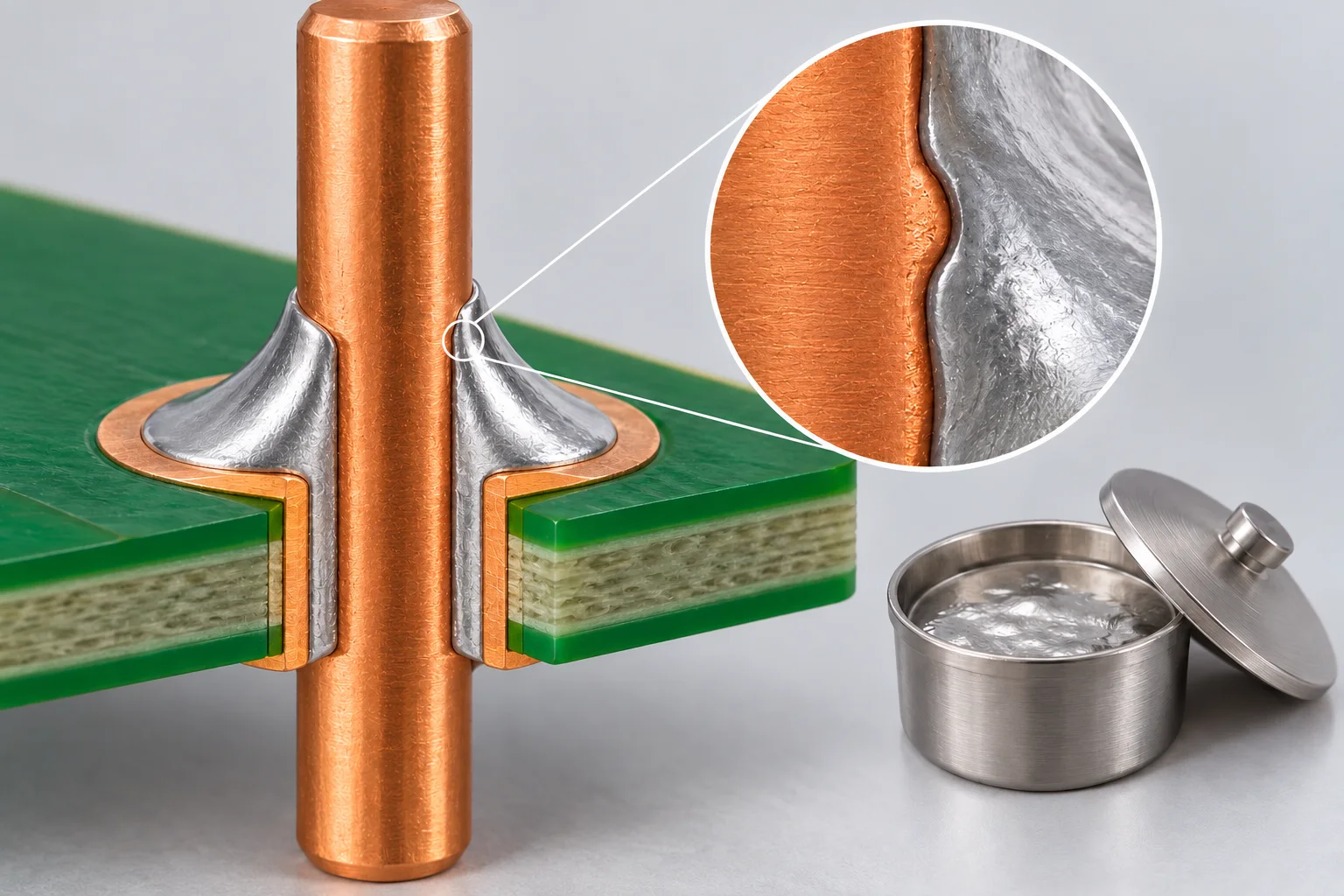
When a PCB solder terminal appears thinner after soldering, establish whether copper base metal was actually lost before diagnosing dissolution. Molten tin-bearing solder can dissolve copper, but appearance may also change with plating, solder coverage or viewing position. Retain unsoldered same-batch controls and correlate geometry evidence with cumulative solder contact and bath-analysis records.
Copper need not melt for dissolution to occur
Kester's technical guidance discusses copper entering molten solder from boards and components and the effect of copper in the alloy on further dissolution. An ACE selective-soldering paper hosted by IPC also discusses copper erosion in relation to alloy, contact time and flow conditions. These support the mechanism, not a universal terminal erosion rate.
The paper's numerical results belong to its particular boards, alloys and equipment. This article adopts no general contact-time limit, rework count, bath temperature or composition threshold. Local loss in PCB barrel copper must not be used directly to predict dimensional loss in a different solid terminal pin.
Compare the same location and material
Identify abnormal pieces and unsoldered same-batch controls, with axial position, section direction and original geometry. In a microsection, distinguish copper base metal, plating, solder and interface regions. A smaller apparent outside diameter or colour change alone does not establish copper dissolution.
Where needed, use a laboratory with an appropriate preparation and analysis method. Preserve scale, preparation records and images. Removing solder or plating can itself alter a surface; do not attribute the entire dimensional change after an unvalidated removal process to soldering. Avoid repeatedly reheating a failure specimen before investigating its original condition.
| Record | Units or content | Purpose |
|---|---|---|
| Terminal and control | Part number, material, finish and batch | Avoid unlike starting geometries |
| Local geometry | mm or μm, location and method | Establish base-metal loss |
| Contact history | s, initial soldering and each rework separately | Retain cumulative exposure |
| Process state | Alloy, temperature °C, nozzle and flow settings | Define comparable conditions |
| Bath analysis | Sampling time, location, batch and concentration units | Link results to the solder actually used |
A supply certificate is not an in-use bath analysis
An original solder certificate describes the delivered material. An operating bath needs sampling records under the applicable process requirements. Link the affected production time to bath sampling, additions and maintenance. An analysis without sampling time or location may not represent the process that produced the part.
Check concentration units: by mass-fraction definition, 1 wt%=10000 ppm, so 0.50 wt%=5000 ppm. This is only a conversion, not a recommended copper concentration or alarm limit. Obtain limits and sampling frequency from the actual alloy supplier, equipment process and approved requirements. Do not improvise elemental additions to correct a bath.
Validate more than appearance
For PCB solder terminals, combine before/after material and dimensional evidence, actual thermal history, contact time and post-process criteria in a controlled investigation. If local base-metal loss is confirmed, review remaining geometry and connection condition against functional risk. Do not reduce allowable current in direct proportion to a dimensional loss.
Terminal solderability tests address wetting and related questions; they do not alone prove that prolonged solder contact preserved base dimensions. Complete the applicable dimensional, soldering and functional checks after process changes.
Questions
Does a low-copper-dissolution alloy remove the need for validation? No. Check its conditions and validate the actual terminal and PCB construction.
Is the bath setpoint enough evidence? Retain relevant measured-temperature evidence, contact history, alloy and flow information as well.
Sources
Kester guidance on lead-free alloys and copper dissolution; IPC-hosted ACE paper on selective soldering and copper erosion.
The AI cover illustrates the copper/solder interface; it is not a Hongchuan terminal section or failure record. No dissolution rate, bath limit, rework allowance or current rating is specified.