


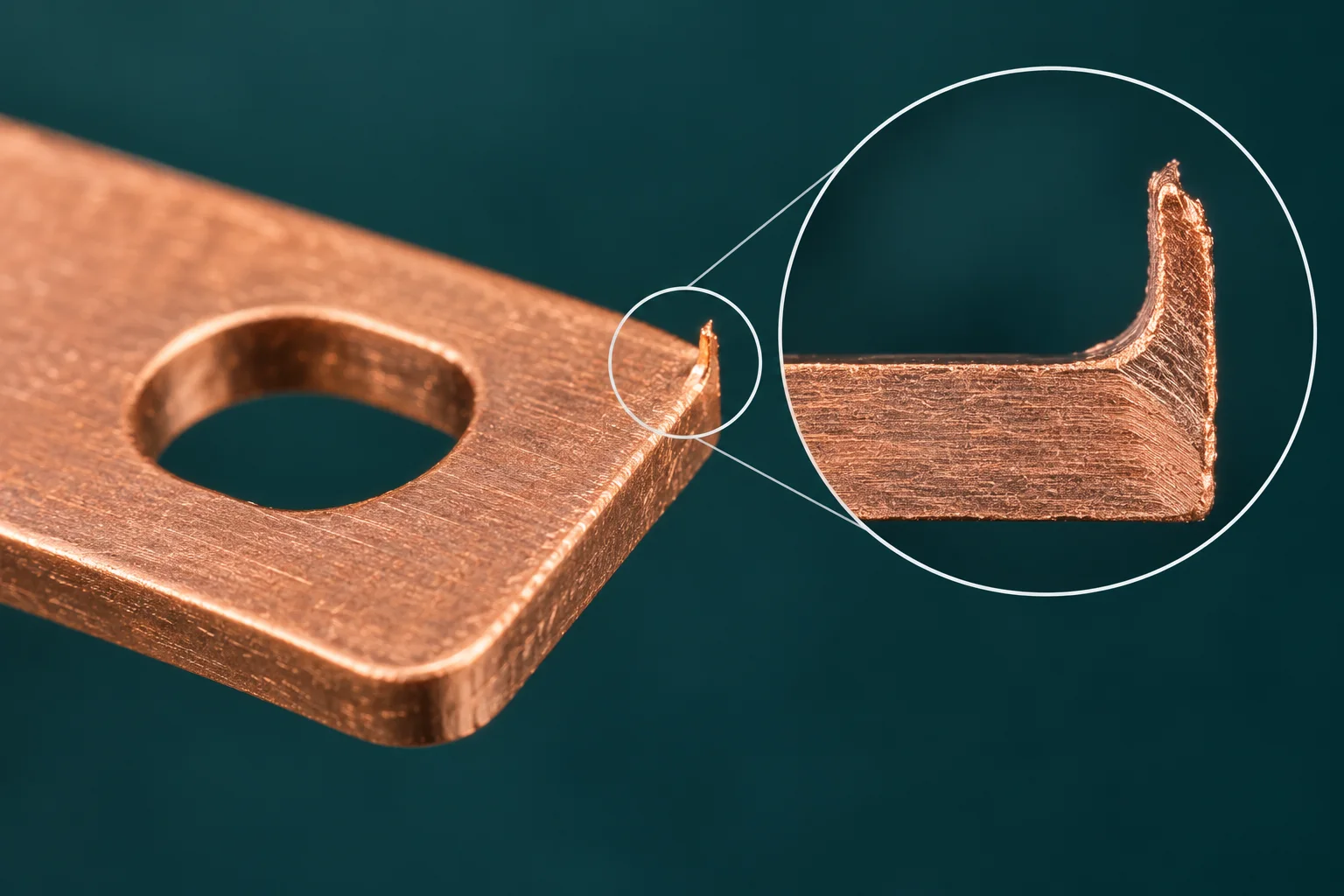
Before accepting a stamped SMD busbar edge, identify the controlled edge, protrusion direction and maximum allowed value. Measure peak height relative to an agreed reference surface and report burr base thickness separately when required. A photograph, touch check or single section is not automatically a whole-part maximum inspection.
Height and base thickness describe different features
KEYENCE's pressing-defect guide distinguishes burr base thickness from height and identifies the other regions of a sheared edge. A projected lateral width must not be reported as height. Roughness over the fracture surface should not automatically be classified as burr protrusion.
| Feature | Suggested definition | Report |
|---|---|---|
| Burr height | Maximum protrusion along an agreed direction from a reference | mm or μm and peak location |
| Base thickness | Width where the protrusion joins the parent material | Section orientation |
| Direction | Orientation relative to PCB, insulation or contact face | Part orientation photo |
| Finished edge | Specified edge geometry after deburring | Chamfer/radius and residual protrusion |
Define the controlled edge on the drawing
The public ISO 13715:2017 description concerns indication of edges of undefined shape. A geometrically defined chamfer requires the applicable dimensioning rules. This article does not reproduce standard symbols or replace the drawing. Mark external edges, hole edges and solder feet that need control, then agree the reference and orientation.
Assess edges near solder pads, insulating films and mating surfaces against their function. There is no general burr-height limit established here for every copper busbar. Define direction in the actual assembly coordinate system rather than calling it simply up or down.
Search the specified area for the highest point
As an inspection proposal, first map the agreed edge region at low magnification, then acquire height or section data at candidate peaks. Save reflection, occlusion and filtering settings for optical methods. For contact methods, verify that the tip and measuring force do not flatten the burr. State the covered location if only one section is measured.
In a hypothetical example, the reference is at 0.012 mm and a local peak at 0.057 mm along the same direction. Relative protrusion is 0.045 mm, or 45 μm. This applies to that location and reference; acceptance still depends on the specified area, tolerance and decision rule.
Reinspect after removal
For SMD busbars, recheck the edge, solder contact area, adjacent dimensions and loose metal after deburring. Copper-aluminum punched-hole interface damage needs its own inspection; a pure-copper burr report does not establish composite-interface integrity.
Frequently asked questions
Is a smooth touch check sufficient?No. It neither quantifies the peak nor replaces a safe agreed inspection method.
Can an image scale establish height?Only when calibration and projection correspond to the required dimension. Three-dimensional protrusions require a suitable height measurement.
Cover image is an AI-generated engineering illustration, not an HC product photograph, laboratory or test record. Hypothetical values are not product specifications or acceptance commitments.