

For a uniform constant-thickness PCB busbar material, sheet resistance Rs is commonly expressed in ohms per square. In an ideal rectangular DC model, Rs=rho/t and end-to-end R=Rs times L/W. Sheet resistance is not the resistance of an entire formed part with holes and joints, and ohms per square does not mean ohms per square millimetre.
Keep the quantities separate
Ossila relates resistivity to sheet resistance and thickness, and describes geometry conditions for four-point measurements. Use resistivity rho in ohm metres and thickness t in metres. The dimensionless L/W ratio gives the number of squares along an ideal rectangular current path.
| Quantity | Unit | Meaning |
|---|---|---|
| Resistivity rho | ohm metre | Material parameter at stated condition and temperature |
| Thickness t | m, or converted from mm | Use consistent length units |
| Sheet resistance Rs | ohms per square | Scale for uniform in-plane conduction |
| Resistance R | ohms, milliohms or microohms | Result between defined endpoints |
A three-square example
Assume rho=1.75 times 10 to the power of minus 8 ohm metres and t=0.50 mm, or 0.00050 m. Rs is then 35 microohms per square. A 30 mm long, 10 mm wide rectangle has L/W=3 and ideal resistance 105 microohms. These are hypothetical inputs, not Hongchuan specifications.
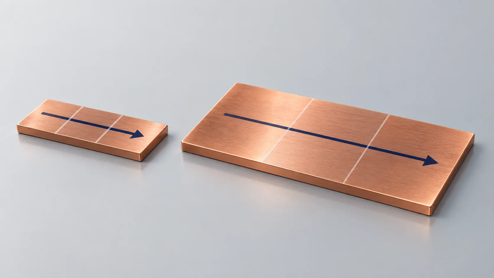
Doubling both length and width to 60 mm and 20 mm, while holding thickness and resistivity fixed, still gives three squares and 105 microohms. Area increases but the ratio does not. The square notation distinguishes a geometric ratio from an area-normalized resistance.
Review the current-entry geometry
The rectangular result assumes uniform material and cross-section with approximately uniform current between complete opposite end faces. A PCB copper busbar fed through small pads, holes or local contacts can have spreading and constriction effects. Necks, holes and joints require an appropriate model or defined measurement, rather than counting squares in the outer outline.
Ossila notes that sample edges, thickness and probe spacing can require corrections. Confirm method applicability before transferring a thin-film four-point formula to a thick copper component.
Specify the reported result
A useful RFQ identifies material condition, thickness, temperature, current-entry regions and voltage taps. Retain geometry corrections for a sheet-resistance result and state whether a finished-part resistance includes solder joints or external contacts. See resistance normalization to 20 degrees C for temperature comparisons. This DC model does not cover high-frequency skin and proximity effects.
Questions
Does larger area always reduce sheet resistance? Not for proportional scaling at fixed resistivity and thickness. Endpoint resistance also depends on geometry and contacts.
Does sheet resistance establish a current rating? Connections, cooling and allowable temperatures still need validation.
Sources
Ossila sheet resistance theory;Ossila measurement guide
The cover is an AI geometry concept. Grid overlays are not machined slots or measured dimensions. All values are hypothetical and establish no material or product guarantee.