


Direct answer Read XRF coating thickness together with substrate, layer stack, point location and calibration range. A stable number does not establish accuracy when the analysis model does not match the part.
Hitachi High-Tech identifies substrate changes, calibration limits and positioning as potential error sources. This guide proposes report checks; it is not a test certificate for a Hongchuan part.
Confirm the layer model
A PCB terminal may use different copper alloys and coating stacks. Confirm any underlayer as well as the tin finish. For copper-aluminum hardware, evaluate each side according to its actual construction.
| Report field | Purpose | If missing |
|---|---|---|
| Substrate and layers | Define the analysis model | Check drawing and material records |
| Point photograph | Identify face, edge and foot | Mark and remeasure |
| Standards and range | Confirm method suitability | Review calibration records |
| Individual readings | Reveal local variation | Retain point and repeat data |
Control positioning
Curves, steps and hole edges complicate focus and spot placement. A beam spanning multiple faces, or movement during acquisition, may not represent the intended area. Check instrument geometry limits and use an appropriate fixture.
Investigate an outlier
Confirm lot and drawing, check the layer model and standards, then repeat at a documented position. Persistent differences may require an alternative method selected by the laboratory. Agree thickness limits, sampling and acceptance rules with the supplier.
Common questions
Does a passing average mean every area passes?
No. Retain location-specific results against the agreed drawing.
Does XRF prove solderability and corrosion performance?
Those properties need separate evidence. See the terminal plating selection guide.
Sources
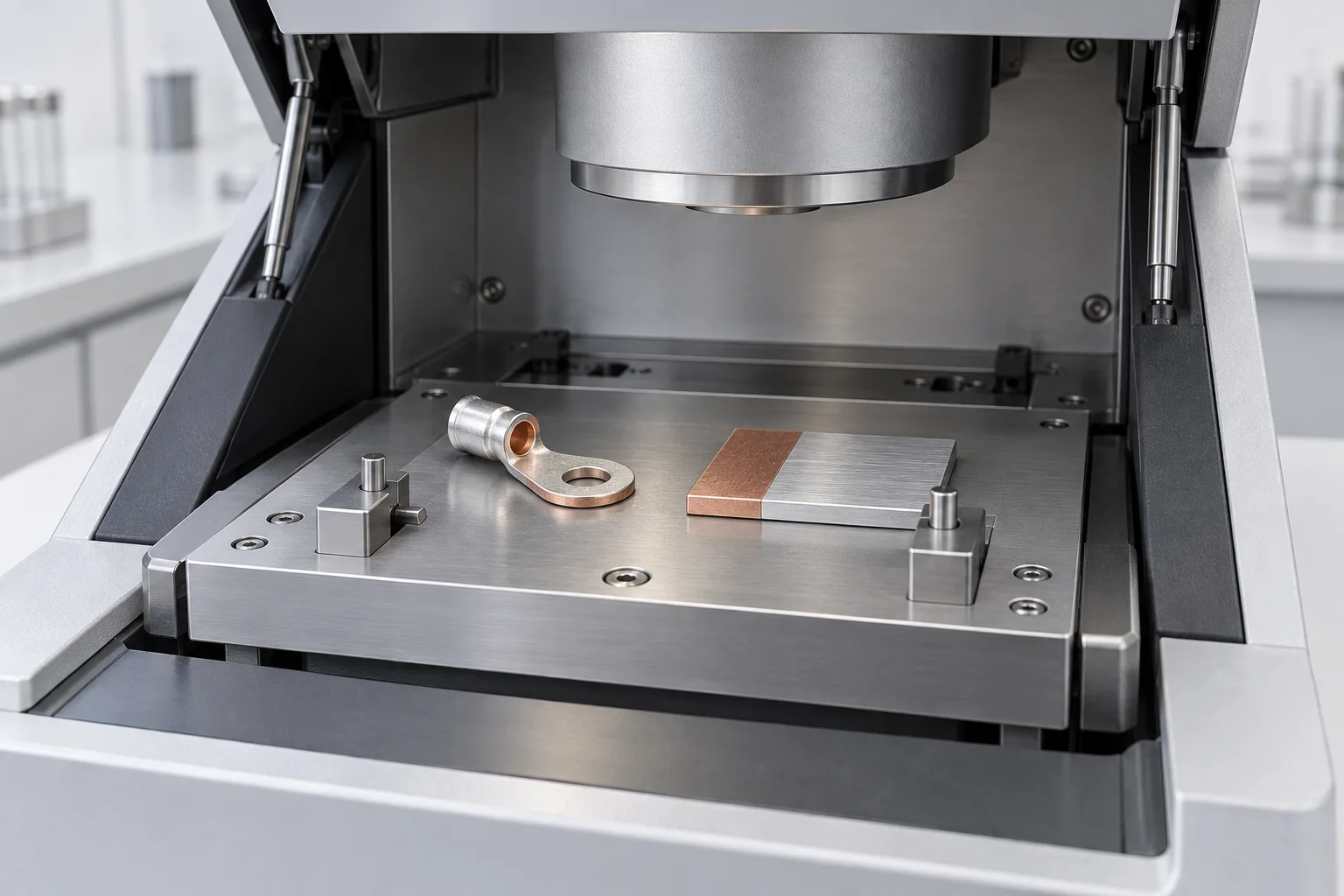
The cover is an AI-generated concept, not a photograph of Hongchuan equipment or an inspection certificate.