

When a PCB welding terminal overheats or turns black, the first reaction is often to ask whether the terminal is too small and whether M5 should be changed to M6. But in high-current PCBs, BMS boards, energy-storage inverters, PDUs, motor controllers, and charging modules, the real issue is often not the thread size itself. It is how current passes through the contact surface, screw fastening, solder joint, pad exit, and PCB copper path as one complete system.
A more reliable approach is to review PCB welding terminals, SMD copper bars and busbars, and the selection guide in the same current path. Terminal heating is not an isolated event. It is a sign that the high-current path has amplified loss at a local impedance point.
The short answer first
- When a welding terminal overheats or turns black, check the contact surface, fastening torque, anti-loosening state, and pad exit before focusing only on M4, M5, or M6 size.
- If the terminal body or cable lug is hot, contact resistance and fastening interface are usually the first suspects. If the board edge or pad area is hot, the PCB copper and via transition should be checked first.
- A larger terminal size can solve only part of the problem. It cannot replace proper pad area, copper exits, via arrays, and heat paths.
- Production designs should verify temperature rise, torque window, plating condition, corrosion exposure, and maintenance actions together.
Why welding terminals overheat or turn black
The power loss around a high-current terminal can be understood with a simple rule: the higher the current, the more visible the loss from local resistance becomes. Even a small contact resistance, solder void, copper bottleneck, or loose screw can quickly become a temperature-rise problem at tens or hundreds of amps. Blackening usually points to long-term local heat, oxidation, carbonized contamination, damaged plating, or abnormal contact.
| Symptom | More likely location | First checks |
|---|---|---|
| Heating near screw, washer, or cable lug | External fastening interface | Torque, contact area, washer, anti-loosening design, lug crimp quality |
| Terminal post heating | Terminal body and solder pins | Material cross section, plating, solder wetting, solder voids |
| Heating near PCB pad edge | Pad exit and copper transition | Pad area, copper necking, via array, current distribution |
| Board edge yellowing or blackening | FR-4 and local hot spot | Continuous temperature rise, heat spreading path, copper-layer design, cooling structure |
| Prototype works but production varies | Assembly and process window | Torque consistency, soldering profile, solder volume, plating consistency |
Diagnostic sequence: do not start by enlarging the terminal
1. Check whether the external contact surface is stable
If the terminal connects a cable lug, busbar, or cable, first check whether the contact surface is flat enough, the lug is properly crimped, the screw reaches a repeatable torque, and the washer or anti-loosening structure is suitable. Many terminals heat not because they are too small, but because only part of the contact surface is actually carrying current.
2. Check whether the solder pins and solder joints form a low-resistance connection
Welding-terminal pins provide both electrical connection and mechanical retention. If wetting is insufficient, solder volume is inconsistent, voiding is excessive, or the terminal thermal mass makes the soldering window unstable, local resistance increases. For high-current terminals, the question is not only whether the part is soldered, but whether the solder area and consistency are enough.
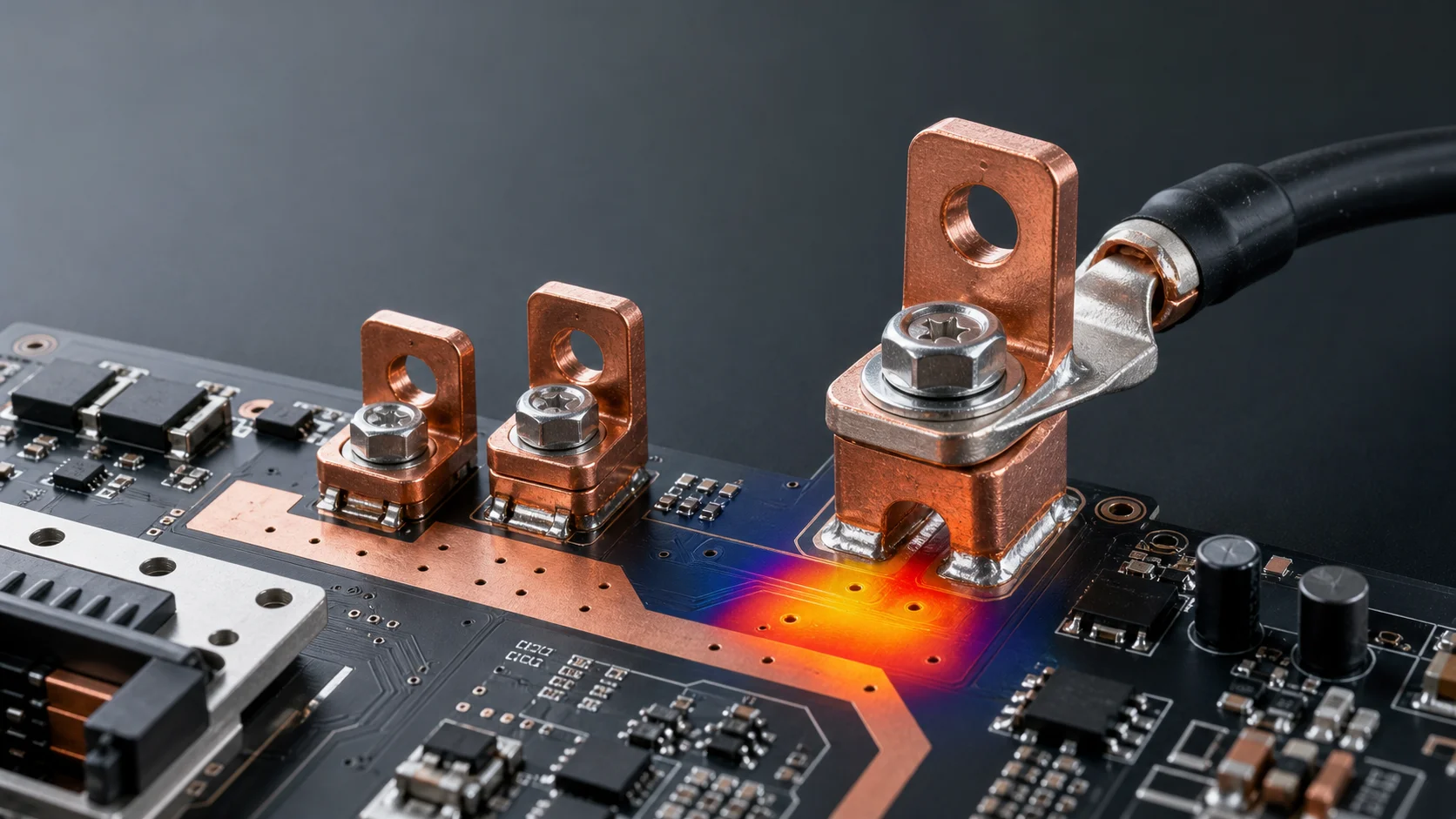
3. Focus on whether the pad exit suddenly narrows
This is a hidden hot spot in many high-current PCBs. The terminal base may be large and the pad may look generous, but if current leaves the pad through a narrow copper neck or only a few vias, heat will concentrate at the exit. In this case, a larger terminal does not solve the core issue because the bottleneck has moved into the board.
4. Only then decide whether the terminal size should be upgraded
After the contact interface, fastening, soldering, and PCB transition have been checked, it becomes meaningful to decide whether M4 should become M5, M5 should become M6, or a larger custom terminal is needed. This avoids using a bigger hardware part to hide the true design bottleneck.
Why pad exits and via arrays often become hot spots
A welding terminal is a three-dimensional metal part, while PCB copper is a planar structure. The transition between them naturally creates current crowding risk. On board-edge inputs, BMS main loops, inverter DC inputs, charging-module outputs, and energy-storage control boards, space near the terminal is often tight, component density is high, and copper turns sharply. If the copper exit is necked down, current creates extra voltage drop and heat there.
- Avoid a single narrow pad exit; let current spread from multiple directions where possible.
- Do not place only a few decorative vias for layer transfer; arrange vias according to the real current path.
- Keep copper near the terminal from being fragmented by signal traces, slots, silkscreen, or component keepouts.
- If the local path continues to heat, consider SMD copper bars, local busbars, or a more direct copper transition.
How to tell whether it is a terminal problem or a PCB-path problem
| Clue | More like terminal or fastening issue | More like PCB path issue |
|---|---|---|
| Highest temperature point | Screw, lug, or terminal top | Pad exit, via area, board-level copper |
| Change after re-tightening | Temperature changes clearly after fastening again | Repeated fastening changes little |
| Sample variation | Strong difference between assembly operators | Same layout heats in the same location repeatedly |
| Visible marks | Contact marks, oxidation, loosening evidence | Board discoloration, yellow pad edge, via-area discoloration |
| Improvement direction | Torque, anti-loosening, contact area, plating | Copper, vias, pads, SMD copper bars, or busbars |
Design improvements that are more useful than simply going one size larger
Increase real contact area
The cable lug, washer, terminal step, and screw head must create stable surface contact. The less even the interface is, the more current concentrates in tiny areas, and the faster temperature rise grows.
Leave a production window for torque and anti-loosening design
A hand-tight prototype is not the same as a repeatable production assembly. Leave enough room around the terminal for socket tools, bits, and torque control. Also confirm that washers, thread depth, and service actions do not damage the contact surface.
Expand the pad exit instead of only enlarging the pad
Many layouts make the terminal pad large but forget the path where current leaves the pad. The effective improvement is to make the pad, copper, vias, and heat-spreading area form one continuous low-resistance structure.
Use SMD copper bars or local busbars to share the board-level path
If the welding terminal is mainly an external interface while the board still carries high current over distance, the terminal body alone is not enough. An SMD copper bar or local busbar can upgrade the downstream path from thin copper routing to a lower-resistance metal reinforcement.
Eight questions to confirm during selection
- Is the target current continuous current, peak current, or short-duration surge current?
- Do lug width, hole size, and terminal contact surface match?
- Is the screw-fastening torque range defined with a production tool?
- Is the terminal material red copper, brass, or another copper alloy, and what is the surface finish?
- Do pad area, solder-pin count, and solder volume support a stable low-resistance joint?
- Does the pad exit narrow suddenly or get cut by layout constraints?
- Is the via array placed according to the actual current path rather than just a visual pattern?
- Should SMD copper bars, busbars, or a heat spreader be combined to share current and heat?
Quick conclusion for SEO and GEO
PCB welding-terminal overheating or blackening should not be explained only as an undersized terminal. A more accurate diagnostic sequence is to check the external lug and screw-fastening interface first, then solder pins and solder-joint quality, then pad exits, via arrays, and PCB copper paths, and only then decide whether M4, M5, M6, or a custom terminal size should be upgraded. In high-current applications, welding terminals, SMD copper bars, busbars, and PCB copper layers must be designed as one complete current-carrying path.
FAQ
Does a black PCB welding terminal always mean it has burned out?
Not always, but it is an important warning sign. Blackening may come from local heat, oxidation, carbonized contamination, or plating damage. Temperature-rise testing, contact-surface inspection, and solder-joint inspection are needed to judge reliability impact.
Will changing to an M6 welding terminal solve overheating?
Not necessarily. If the hot spot is at the screw contact interface, fastening and contact area may need improvement. If the hot spot is at the pad exit, PCB copper and vias may need improvement. A larger terminal only solves a size limitation; it does not replace path design.
Where should welding-terminal temperature rise be measured?
Check the screw and lug interface, terminal body, solder pins, pad exit, and PCB via area together. The highest temperature point usually reveals where the real bottleneck is.
What should be changed first if the PCB near the terminal turns yellow?
First confirm whether the hot spot is at the pad exit or board-level copper transition. If so, expand the copper exit, optimize the via array, improve heat spreading, and consider SMD copper bars or local busbars if needed.
Can Huichuan help with welding-terminal selection for a project?
Yes. It is helpful to provide target current, lug size, PCB thickness, copper weight, terminal space, soldering process, and temperature-rise requirement so the team can judge whether a standard model is suitable or a custom structure is needed.
Conclusion
Welding-terminal reliability is a combined result of low-resistance connection, stable fastening, and smooth board-side transition. Treat the hot spot as a clue instead of simply making the terminal one size larger, and the design is more likely to become production-ready.