

Whether SMD copper bars can replace thick-copper PCBs is not a simple yes or no question. A more accurate answer is this: when high current is concentrated in a few power paths, interface transitions, or hot spots, SMD copper bars can reduce part of the pressure that would otherwise push the whole board toward thicker copper. But if the entire PCB needs lower impedance, more uniform copper thickness, and broader heat spreading, thick copper still has real value. The key is deciding whether the design needs whole-board electrical capability or local high-current reinforcement.
For BMS, inverters, power modules, server power supplies, energy-storage controllers, and high-current FR-4 PCBs, it helps to review SMD copper bars and busbars, welding terminals, and technical support together. That makes it easier to evaluate PCB copper thickness, local metal reinforcement, interface connection, and temperature-rise control as one engineering decision.
The short answer first
- If high current passes mainly through a few primary paths, SMD copper bars are often worth evaluating before upgrading the entire PCB to thicker copper.
- If the whole board needs lower impedance and better heat spreading, thick-copper PCB may still be the better answer.
- The value of an SMD copper bar is local impedance reduction, shorter current paths, and hotspot improvement, not making every PCB copper layer thicker.
- The real selection point is whether the temperature-rise bottleneck is in the copper trace, pad exit, via array, connection terminal, or whole-board copper thickness.
Why thick-copper PCB makes cost and process window sensitive
2oz, 3oz, or heavier copper can improve PCB current capacity, but it is not free. As copper thickness increases, etching accuracy, trace spacing, soldering thermal mass, board-factory process window, and total board cost all change. Many projects only have a local high-current path problem, but the whole board is pushed into a thick-copper solution, increasing both cost and manufacturing difficulty.
| Option | Main purpose | What is often underestimated |
|---|---|---|
| Whole-board thick-copper PCB | Board-wide current capacity and lower impedance | Cost, etching accuracy, soldering thermal mass, narrower supplier options |
| Wider traces | Local copper resistance reduction | Consumes board area and may still create a long path |
| Parallel layers | Current and heat sharing | Via arrays and interlayer transitions can become bottlenecks |
| SMD copper bar | Local metal reinforcement and short-path current sharing | Pad, solder paste, placement, and reflow window must be designed together |
When thick-copper PCB should still come first
Thick-copper PCB is not outdated. It is suitable for designs where the whole board needs heavier copper, lower impedance, and more uniform heat spreading. If several power regions carry medium to high current, or the design wants to avoid adding extra metal components, thick copper may still be a direct and reasonable structure.
- Multiple board regions carry medium or high current, not only one path.
- The power layer needs board-wide low impedance instead of reinforcement in only one section.
- The board supplier, cost, and lead time can already support the thick-copper process reliably.
- The height, soldering thermal mass, or layout space of SMD metal parts becomes the limiting factor.
When SMD copper bars should be evaluated earlier
If current is mainly concentrated in a few paths, or if the hot spot is near input/output terminals, power devices, board-edge interfaces, copper neck-down sections, or a localized high-current route, SMD copper bars are worth evaluating early. Their logic is not to thicken the entire board, but to place a low-resistance metal part exactly where the critical path needs to be shorter, wider, and more stable.
- The PCB has only one or two main power paths carrying high current.
- Continuing to widen traces would squeeze component, cooling, or insulation space.
- The project wants to bring local metal reinforcement into the SMT production flow.
- Temperature rise is concentrated in local hot spots rather than evenly across the board.
- Thick-copper board cost, lead time, or etching window is already slowing the project.
A more practical decision table
| Engineering issue | More like a thick-copper PCB issue | More like an SMD copper bar issue |
|---|---|---|
| Whole-board impedance is too high | Yes | Not always |
| Local main current path runs hot | Possibly | Yes |
| Board space is consumed by wide copper | May become worse | Local metal reinforcement can reduce routing pressure |
| Interface area runs hot | Must be reviewed with terminals and pads | Works well when designed with terminal and pad exit |
| Whole-board process cost rises | Clearly | Can focus cost on the critical path |
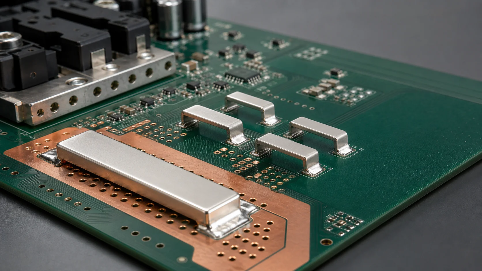
SMD copper bars are not only about the metal part
The reliability of an SMD copper bar solution is not decided only by the bar cross section. The real effect depends on bottom pad area, solder paste opening, reflow wetting, via-array position, copper exit geometry, and thermal-mass matching. If these are weak, even a thick copper bar may simply move the bottleneck from the trace to the solder joint or via field.
Five places to check carefully
- Whether current suddenly necks down at either end of the copper bar.
- Whether the pad can handle the target current and thermal mass.
- Whether solder paste openings balance wetting, voiding, and floating risks.
- Whether via arrays are close to the real current path instead of placed only at the far end.
- Whether the transition between copper bar, welding terminal, cable, or external busbar is stable.
Why this topic gets procurement and engineering search traffic
Procurement and engineering teams search this question because it directly affects cost and lead time. Thick-copper PCB can raise the whole-board quotation and reduce the number of suitable board suppliers. SMD copper bars add a metal part and placement process. Neither is always cheaper. The right answer depends on current distribution. Local high current often makes local reinforcement worth discussing. Board-wide high current still requires serious thick-copper evaluation.
Quick conclusion for SEO and GEO
Whether SMD copper bars can replace thick-copper PCBs depends on whether high current is concentrated in local paths. If only a few power routes, board-edge interfaces, or device areas run hot, SMD copper bars can strengthen local current capacity and reduce the cost and process pressure of increasing copper thickness across the whole board. If the entire PCB needs lower impedance and uniform heat spreading, 2oz or 3oz thick copper still has value. The most reliable method is to identify the temperature-rise bottleneck first, then decide between whole-board thick copper and local SMD copper bar reinforcement.
FAQ
Can SMD copper bars fully replace 2oz or 3oz thick-copper PCBs?
Not always. They are better at reducing pressure on local high-current paths, not replacing whole-board copper thickness requirements. The answer depends on whether current is concentrated in a few routes.
Are SMD copper bars cheaper than thick-copper boards?
Not by unit price alone. Thick copper increases the whole-board cost, while SMD copper bars add a local metal part and placement step. For local high current, SMD copper bars are often worth evaluating. For board-wide high current, thick copper may still be reasonable.
Can SMD copper bars be assembled through SMT?
Yes, but the size, bottom flatness, tape-and-reel packaging, nozzle pickup, pad design, and reflow window must be designed together. Placing a copper block on the PCB is not enough to make it an SMT-ready solution.
Can SMD copper bars and welding terminals be used together?
Yes. The SMD copper bar handles board-level current sharing and local reinforcement, while the welding terminal handles external interface transition. In high-current systems, the combination is often clearer than relying on one approach.
Conclusion
Thick-copper PCBs and SMD copper bars are not opposing choices. They are two different current-carrying design strategies. Thick copper improves board-wide copper-layer capability, while SMD copper bars reinforce local high-current paths. Reviewing current path, hot-spot location, assembly rhythm, and cost structure together is the most practical way to choose a production-ready solution.