

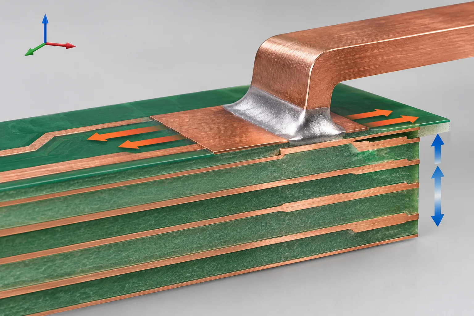
A PCB busbar thermal model should retain separate in-plane and through-thickness effective conductivities and their material coordinates. A multilayer copper-and-dielectric board may be simplified as orthotropic. Neither bulk copper conductivity nor a tutorial board value is a universal property of the complete PCB.
Distinguish the heat paths
Ansys Icepak compact PCB objects use directional conductivities. COMSOL also demonstrates an anisotropic board to represent the different conduction paths of dielectric layers and copper traces. These are effective board properties; model the busbar, solder and interfaces separately.
| Field | Meaning | Evidence |
|---|---|---|
| In-plane conductivity | Along board, W/(m K) | Stackup, copper distribution and averaging |
| Normal conductivity | Across thickness, W/(m K) | Dielectric, layers and via structures |
| Material coordinates | Directions relative to the board | Definition and rotation |
| Local path | Pads, neck-downs and vias | Layout and required spatial scale |
Identify the thickness axis first
Global z is not always board thickness. The Ansys example places the board in the x-z plane, making y normal to it. Verify material orientation after rotating geometry. COMSOL PCB material-data guidance likewise associates the directional properties with the board coordinate system.
Keep a local-axis sketch and name the thickness direction. A list of kx, ky and kz alone does not let a reviewer establish physical orientation. Equal units do not make the three entries interchangeable.
Assess local limits of homogenization
A homogeneous board reduces model cost. Near an SMD copper busbar joint, assess whether it hides copper discontinuities, neck-downs or via placement. Good average lateral conduction does not establish an effective path from a particular joint to rear-side cooling.
Define whether the question concerns whole-board cooling or local connection temperature before selecting uniform, regional or detailed representation. Spatially varying material data derived from PCB structure are another available approach, still requiring validation for the actual layout.
Retain the assumptions when comparing designs
Archive board and layer thicknesses in mm, copper coverage and connectivity, property sources, temperature conditions and averaging method. Check sensitivity to important assumptions and compare with physical temperature measurements. Review temperature and convection boundaries separately from material direction.
Questions
Does one FR-4 k value describe the board? Establish whether it describes dielectric or the copper-containing composite, and in which direction.
Must rear copper lower busbar temperature? The through-board path, interfaces and cooling boundary still determine the result.
Sources
Ansys Icepak compact PCB model;COMSOL anisotropic PCB tutorial;COMSOL PCB material data and coordinates
The cover is an AI composite-board concept. Layer thickness and arrows are not to scale and show no computed temperature field. No Hongchuan thermal property or product rating is stated.