


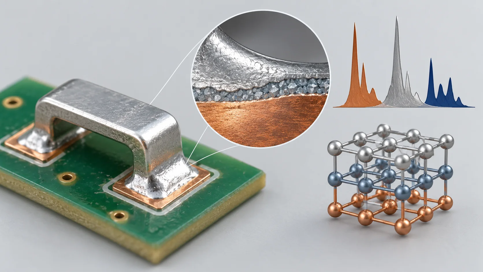
Cu and Sn peaks in EDS from a surface mount PCB jumper solder joint support elemental evidence under the stated conditions. Those peaks alone do not establish a particular Cu-Sn intermetallic phase. Review location, quantification and suitable structural evidence, distinguishing measured results from candidate interpretations.
Define the analytical question
Oxford Instruments describes EDS as elemental and chemical analysis. Its EDS/EBSD integration guidance distinguishes chemical information from crystallographic information and explains their combined use in phase identification. Element presence, composition and structure answer different parts of the question.
| Evidence | Supports | Retain limitations |
|---|---|---|
| EDS spectrum and map | Element signals and distribution | Capability, overlapping peaks and quantification |
| Composition | Reported weight or atomic percentages | Unit and analysed region |
| Diffraction or crystallography | Suitable structure and candidate-phase matching | Preparation, database and match quality |
| Section-location image | Physical layer or region analysed | Whether the target layer is covered |
Locate the analysis region
For a surface mount PCB jumper joint, mark substrate, finish, solder and interface. A nominal point analysis still samples a finite signal-producing region. Contributions from neighbouring materials may produce a mixed result, which should not automatically be named as one phase. The laboratory should assess spatial applicability for the equipment, voltage and sample.
Retain accelerating voltage in kV, preparation, location images, spectra and quantification settings. No universal penetration depth is proposed here. See jumper microsection plane and target location for section selection.
Keep ratios and phase assignments distinct
Weight percent and atomic percent are different quantities. Peak heights alone do not give a compound atomic ratio. A proposed Cu6Sn5 assignment should state supporting evidence and unresolved alternatives.
EDS can contribute to phase analysis by narrowing candidates. Combine appropriate chemical, crystallographic, location and morphology evidence. The laboratory should choose complementary methods for the layer size and sample condition; no single diffraction test is mandatory for every joint.
Request an auditable conclusion
Define whether the task is contamination screening, interface composition or phase identification before commissioning analysis. Report observations, interpretations and unexamined items separately. Phase presence alone does not establish failure; morphology, thickness, performance and acceptance criteria remain relevant.
Questions
Can an automatic compound label settle acceptance? Review the database, location and supporting evidence.
Does near-stoichiometric composition prove a single phase? Consider mixed sampling and method applicability before excluding alternatives.
Sources
Oxford Instruments EDS overview;Oxford Instruments EDS and EBSD integration
The cover is an AI analytical concept. Peaks, layer thickness and lattice are neither measurements nor a real structure of a specified phase. No Hongchuan failure record is shown.