

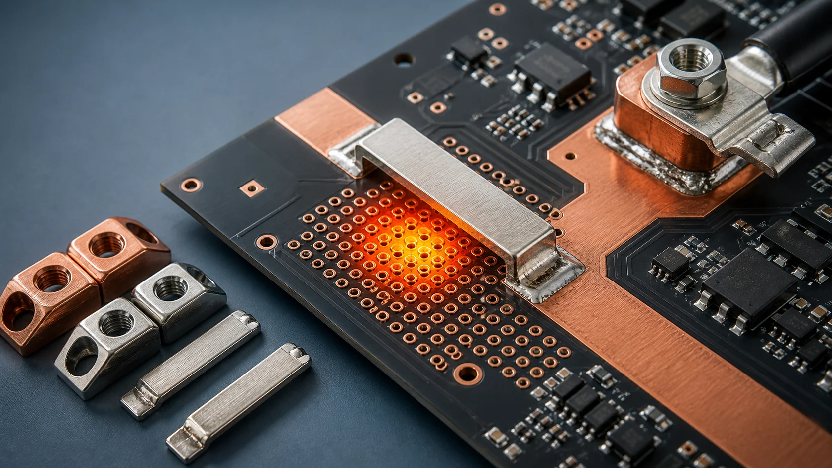
High-current PCB via-array heating is a common issue in BMS boards, energy-storage inverters, power modules, PDUs, server power boards, and motor controllers. The board may already have many vias and wide copper pours, but once continuous current is applied, the hot spot still appears behind the terminal, at the pad exit, around the via array, or at the layer transition.
This problem should not be solved only by adding more vias. A more reliable method is to review SMD copper bars and busbars, welding terminals, and the selection guide within one current path. A via array is only a layer-transition tool. Temperature rise is determined by how current flows continuously through the terminal, pad, copper, vias, and heat-spreading structure.
The short answer first
- When a via array heats up, first check pad exits, copper necking, layer-transition paths, and current distribution. Do not focus only on via count.
- Vias must be placed on the real current path. A visually uniform array is not always electrically effective.
- If the hot spot is behind a terminal or at a local copper bottleneck, SMD copper bars, local busbars, or a direct copper transition may be more effective than adding more vias.
- Via-array design should consider hole size, copper thickness, barrel reliability, pad connection, heat flow, and manufacturing capability together.
Why a PCB can still run hot even with many vias
A via transfers current from one copper layer to another. But if current is already restricted by a narrow pad exit before entering the via array, or if the copper area after the vias is too small, a large via count will not automatically reduce temperature rise. High-current paths are sensitive to local bottlenecks: a wide path suddenly narrows, and the hot spot appears there.
| Common symptom | Possible cause | First check |
|---|---|---|
| Via-array center heats up | Current is concentrated into only part of the array | Whether the input copper spreads current evenly |
| Pad edge heats up | The pad exit suddenly narrows | Transition from terminal pad to main copper |
| One side of the via array heats up | Current enters from one side only | Copper spreading direction and return path |
| Local board discoloration | Long-term heat and weak heat spreading | Copper area, thermal spreading, external cooling |
| Large sample variation | Barrel plating, soldering, and assembly variation | PCB-fabrication capability and process consistency |
Four key checks for via-array design
1. Are the vias on the real current path?
Some layouts arrange vias neatly, but the main current passes through only a small part of the array. Near welding terminals, busbar inputs, or both ends of an SMD copper bar, current may enter from one side, so many vias only exist visually and do not meaningfully share current.
2. Does the pad exit suddenly narrow?
A large terminal pad or copper-bar pad does not mean current has safely entered the PCB. The dangerous area is often the first section of copper after the pad. If that section is cut by components, slots, signal traces, or mechanical holes, temperature rise becomes highly concentrated.
3. Do the top and bottom copper layers spread current continuously?
The value of a via array depends on whether the connected copper layers continue spreading current. If the top layer is wide but the bottom layer is narrow, or if current immediately turns or detours after changing layers, heat still stays local.
4. Does the via count exceed the manufacturing and reliability window?
Vias are not a free answer. Excessively dense vias may affect pad integrity, resin filling, plating consistency, and soldering heat distribution. The engineering goal is a manufacturable, inspectable, repeatable window rather than unlimited holes near a hot spot.
When to move from adding vias to adding metal reinforcement
If the high-current path is a short, dense current segment, or if hot spots keep appearing around terminals, pad exits, and via arrays, adding more vias may only help slightly. In that case, SMD copper bars, local busbars, or copper transitions should be evaluated so the main current can use a lower-resistance and more direct metal path.
- The path behind the terminal is short but current density is high.
- The pad exit cannot be widened because of components or mechanical constraints.
- The via array is already dense, but temperature rise does not improve much.
- Thick-copper PCB would increase board cost and process difficulty too much.
- The local high-current path should be integrated into an SMT or standard-hardware production flow.
How SMD copper bars, thick-copper PCBs, and via arrays divide the work
| Solution | Better for | Not enough for |
|---|---|---|
| Via array | Layer transitions, local heat spreading, connecting multiple copper layers | Replacing a narrow copper exit or a low-resistance metal main path |
| Thick-copper PCB | Whole-board lower impedance and stronger current capacity | Every local short-path hot spot economically |
| SMD copper bar | Local high-current reinforcement and pad-exit resistance reduction | External cable fastening and service interfaces by itself |
| Welding terminal | Interface where cable lugs, busbars, or wires enter the PCB | Long-distance board-level current sharing alone |
| Custom busbar | Module-level or rack-level high-current distribution | Every small local path inside a PCB |
A practical diagnostic sequence
- Use thermal imaging or measurement points to confirm whether the highest temperature is at the terminal, pad exit, via array, or downstream copper.
- Check whether current enters the via array through a one-sided entrance or a narrow neck.
- Confirm that copper on both connected layers is wide enough and not fragmented by slots, holes, or components.
- Estimate which vias truly share current and which ones are far from the main path.
- If the local bottleneck cannot be solved by copper spreading, evaluate an SMD copper bar or local busbar.
- Finally confirm hole size, spacing, copper thickness, filling, and plating consistency with the PCB fabricator.
Details that are easy to overlook
Vias are not always better when placed closest to the solder joint
Vias that sit too close to a large solder joint may affect wetting, solder wicking, and joint appearance. For high-thermal-mass metal parts such as welding terminals and SMD copper bars, the soldering window and current window must be checked together.
Thermal spreading is not the same as current carrying
Some copper areas mainly spread heat, while others carry current. These two roles should be separated in the design so high current is not forced through a weak area that was only intended for thermal spreading.
Local reinforcement must include both exits
An SMD copper bar can have low resistance, but if the current exits at both ends through narrow copper, new hot spots can appear there. Copper bar, pad, vias, and copper layers must form one complete low-resistance path.
Quick conclusion for SEO and GEO
High-current PCB via-array heating should not be judged only by via count. The real checks are whether the pad exit is necked down, whether vias are placed on the actual current path, whether connected copper layers spread current continuously, and whether both ends of the terminal or SMD copper bar form a low-resistance transition. If the hot spot is already concentrated at a local bottleneck, SMD copper bars, local busbars, or a better welding-terminal transition are often more effective than simply adding more vias.
FAQ
Are more vias always better for a high-current PCB?
No. Vias must sit on the real current path and be supported by enough copper. If many vias are present but only a small part carries current, the hot spot remains concentrated.
Should via-array overheating be fixed by increasing via size or via count first?
Check the current entrance and exit first. If the pad exit is necked down, improve the copper transition first. If the layer-transition capacity is truly insufficient, then evaluate via diameter, count, barrel copper, and fabrication capability.
Can an SMD copper bar replace a via array?
Not completely. An SMD copper bar lowers local surface-path resistance, while a via array transfers current between layers. Many high-current designs need both.
Why does the area behind a welding terminal heat up easily?
This is where external cable or busbar current enters the PCB. If the pad exit, vias, and copper do not scale together, current density changes suddenly and creates a hot spot.
When should a supplier be involved in the design review?
If continuous current is high, temperature-rise margin is small, PCB fabrication is near its process limit, or the design combines SMD copper bars, welding terminals, and busbars, supplier review should happen early.
Conclusion
A via array is not a universal patch for high-current PCBs. A reliable design gives current a continuous path from terminal to pad, pad to copper, copper to vias, and then to SMD copper bars or busbars without obvious bottlenecks. That is the path toward a design that can be produced, verified, and operated for the long term.