

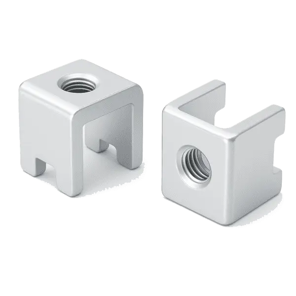
When a high-current terminal gets hot, the first assumption should not be that one part is simply bad. A better starting point is the current path: has contact resistance increased, is tightening torque stable, is the solder area large enough, has the plating or surface condition changed, and does the heat have a path to leave the joint? In high-current PCB connections, overheating is often caused by electrical contact, mechanical fastening, solder transition, and thermal path problems acting together.
If a project already shows high terminal temperature rise, a hot screw joint, discoloration near the pad, or higher temperature after service, it is useful to review the welding terminal page, the SMD busbar page, and the technical support page together. The terminal is only one node in the path. The real question is whether the whole high-current route is continuous, low resistance, thermally manageable, and serviceable.
Check the current path first, not only the terminal appearance
Terminal heating is usually caused by higher local resistance or poorer local heat dissipation. A clean-looking part is not proof of stable contact. A terminal that appears large enough is also not proof that the pad, screw, copper area, and mating part can carry the same current safely.
- First identify where the heat starts: at the screw joint, the solder transition, the PCB copper, or the external cable connection.
- Then check whether the temperature rise changes with current, service cycles, vibration, humidity, or production batch.
- Review the contact surface, tightening force, solder wetting, plating condition, and thermal path.
- Finally decide whether this is a process issue, an assembly issue, or a structural current-capacity limit.
Common causes and what to check first
| Possible cause | Typical symptom | Check first | Improvement direction |
|---|---|---|---|
| High contact resistance | Local heat at the interface, often changing after service | Flatness, oxidation, contamination, and contact pressure | Improve contact area, surface condition, and clamping method |
| Unstable tightening torque | Different temperature rise within the same batch, worse after vibration | Screw size, torque window, washer, and anti-loosening design | Define assembly torque and locking method |
| Insufficient solder area | Heat near the pad or high stress around solder joints and vias | Pad size, solder volume, wetting, and thermal mass | Increase solderable contact area or adjust terminal geometry |
| Narrow copper or bus path | The PCB path heats before the terminal body | Copper thickness, trace width, via array, and corners | Use a shorter, wider path or add an SMD busbar |
| Damaged plating or surface | Contact stability drops after rework or service, with local discoloration | Tin or nickel surface, scratches, contamination, and corrosion risk | Control assembly friction and service environment |
Why the same terminal size can produce different temperature results
Many discussions focus on the current rating of the terminal, but real temperature rise also depends on the PCB, pad, mating part, and assembly condition. The same terminal can behave very differently with different board thickness, copper thickness, pad design, and thermal environment.
1. Terminal current capacity is not the same as system current capacity
The terminal material, thickness, and contact area are only part of the answer. Current also passes through solder joints, pads, copper areas, vias, cable terminals, or external busbars. If any section becomes the bottleneck, heat will concentrate there.
2. Torque and contact area change the real contact resistance
If a screw is too loose, contact pressure is not enough. If it is too tight, the contact surface, thread, or board-level structure can be damaged. Engineering teams need a stable torque window and repeatable contact state, not a one-time sample result.
3. The solder transition is often underestimated
For a welding terminal, the solder joint is not only a mechanical fixing point. It is the key transition where current enters the PCB. A small pad, mismatched thermal mass, poor wetting, or weak via distribution can all increase local temperature rise.
When a different current-carrying structure is needed
If the issue is only process variation, cleaning the contact surface, optimizing torque, and adjusting the pad may help. If the heat comes from a structural bottleneck, the current-carrying solution should be reconsidered.
- If heat concentrates in the PCB copper or via area, consider shortening the path, widening the copper area, or using an SMD busbar to share current.
- If heat concentrates at the external interface and board transition, evaluate a welding terminal that better supports fastening, service, and soldering window requirements.
- If the product requires repeated service, focus on locking structure, anti-loosening design, and contact-surface wear instead of only one temperature-rise test.
- If space is limited, design the terminal, busbar, pad, and thermal structure as one system from the beginning.
A practical troubleshooting checklist
- Record test current, test duration, ambient temperature, and measurement points instead of relying on touch.
- Compare first articles, production parts, and serviced samples to see whether the issue follows assembly condition.
- Check the contact surface for oxidation, contamination, burrs, dents, or plating damage.
- Review tightening torque, screw size, and anti-loosening requirements.
- Inspect solder wetting, solder volume, pad size, and via array against the real current path.
- Find the bottleneck section by section, instead of replacing the terminal while ignoring the PCB and mating part.
FAQ
Does terminal heating always mean the terminal is too small?
No. Undersizing is one possible reason, but contact resistance, tightening torque, solder area, PCB copper path, and thermal conditions all affect temperature rise. The whole current path should be checked together.
Will tightening a screw terminal more always reduce temperature rise?
No. Proper contact pressure helps, but excessive tightening can damage the thread, contact surface, or board-level structure. A repeatable torque window and locking method are more reliable.
Should I use a welding terminal or an SMD busbar to solve overheating?
It depends on where the heat starts. If the issue is at the interface transition and service joint, a welding terminal is worth evaluating first. If the issue is the PCB high-current path or copper bottleneck, an SMD busbar is usually more helpful.
Conclusion
High-current terminal heating is not a single-part problem. It is the result of electrical contact, mechanical fastening, solder transition, and thermal path design working together. Find the hot spot first, then check the current path section by section. That is usually more effective than simply choosing a larger terminal, and it is more likely to lead to a design that can be repeated in production.