


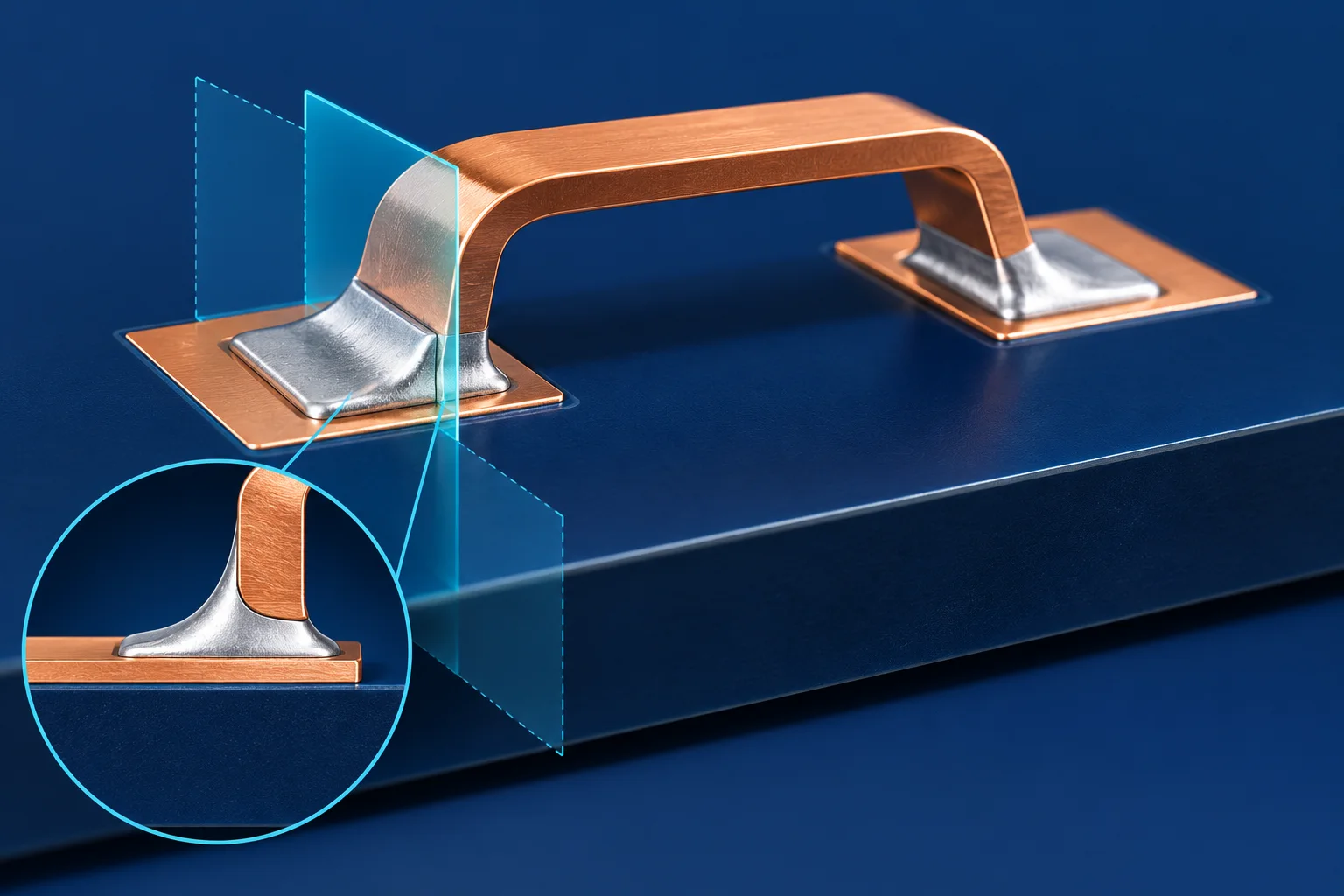
Before microsectioning a surface mount PCB jumper, identify the target soldered foot, section direction and location on an assembly drawing or photograph. A section through the unsupported center of a bridge jumper does not establish the solder condition underneath either foot. Report the plane actually examined.
Locate the target before cutting
CALCE describes locating a failure site before potting, cutting or grinding to the area of interest, followed by polishing and analysis. For a PCB jumper, retain exterior and appropriate electrical observations before selecting the interface to examine.
Struers emphasizes controlled removal to reach a target and describes damage that cutting, mounting and polishing can introduce. Have the laboratory adapt its procedure to the actual jumper assembly. Parameters from a different component are not a universal jumper preparation specification.
Make the section request reproducible
| Item | Suggested record | Avoid |
|---|---|---|
| Sample identity | Board, location, batch and test state | Only “jumper sample” |
| Target | Foot, datum and direction | Unspecified “center section” |
| Final plane | Location image, coordinates or datum distance | Substituting the saw-cut position |
| Image | Scale bar, orientation and analysis method | Unlabelled cropped image |
| Acceptance basis | Drawing or procedure and revision | Invented universal void/crack limits |
Material is removed after sawing, so the final polished plane can differ from the original cut. A reported solder thickness or gap must refer to that plane and a defined measuring direction. Grinding beyond the target cannot recover the lost plane; document the loss and reassess other samples.
Check preparation artifacts
Soft-metal smearing, relief between materials and embedded abrasive can complicate interpretation. Review original images, preparation records and adjacent locations before assigning a cause to a thin line or blank region. Ask the laboratory to resolve ambiguity using an appropriate method.
A microsection is a local, destructive observation. Finding no defect in one section supports a statement about that plane and method, not every joint in a batch. Void area on one section is not automatically the three-dimensional void-volume fraction of the whole joint.
Connect the request to inspection planning
For surface mount PCB jumpers, provide land geometry, assembly orientation, the investigation question and sample quantity. Agree whether multiple sites or adjacent sections are needed. The X-ray void-area and ROI guide also explains observation boundaries; percentages from different methods are not interchangeable.
Questions
Can one good section release the batch? Follow the agreed sampling and acceptance plan; one local image is not a batch procedure.
Is magnification alone sufficient? Preserve a scale bar, location and orientation, especially when images are resized.
References
CALCE microsectioning; Struers microelectronics preparation.
The cover is an AI section-planning illustration, not a micrograph, Hongchuan failure sample or acceptance record. Layer thicknesses are not measurement evidence.