


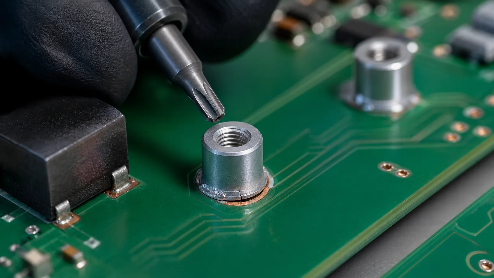
Quick answer: A lifted pad, annular crack or fractured solder joint around an SMT nut after screw tightening is rarely just a weak-nut problem. The load path starts at tightening torque and assembly side load, passes through the nut base and solder joint, and concentrates at the pad copper, solder-mask opening and PCB laminate. Troubleshooting should combine the fastening tool, target torque, PCB thickness, pad anchoring, solder-paste distribution, reflow quality, pull/shear strength and post-thermal-cycle retesting.
Questions answered on this page
- Why does an SMT nut lift the PCB pad or create an annular crack after tightening?
- Can M2, M3 or M4 SMT nut torque be copied from a conventional metal nut specification?
- How do PCB thickness, copper thickness and solder-mask opening affect mechanical strength?
- Which cross-section and strength checks are needed when the nut remains attached but the pad is damaged?
- How should repeated assembly, vibration and thermal cycling be validated for production?
Engineering summary
- Allowable fastening load is controlled by the thread, nut base, solder joint, pad copper and PCB laminate together.
- Pad lift usually involves copper-to-laminate separation, while annular cracking commonly appears in solder, at the mask boundary or around a concentrated load path.
- Driver peak torque, off-axis downforce and abrupt stopping can be more damaging than the programmed torque value alone.
- More solder paste does not automatically add reliability; an excessively thick or uneven solder layer can increase tilt and stress.
- Acceptance should combine visual inspection, thread gauges, tightening torque, pull/shear tests, cross-section analysis and post-environment retesting.
Application context
Engineering issues such as “SMT nut pad lift”, “SMT nut tightening crack”, “M3 SMT nut detached after torque” or “annular crack around PCB nut” usually appear during mechanical assembly, pilot production or reliability testing. Replacing the nut with a larger size may not remove the root cause because the weak interface can be the PCB pad and laminate.
Hongchuan Precision Hardware supplies SMT nuts, SMD busbars, PCB welding terminals and copper-aluminum connectors for high-current PCB hardware applications. This guide is intended for mechanical, hardware, PCB, SMT, assembly and quality teams.
Separate four common failure modes first
| Failure mode | Typical evidence | First checks |
|---|---|---|
| Lifted copper pad | Nut and part of the pad rise from the laminate | Copper peel strength, pad anchoring, rework heat, side load |
| Annular solder crack | Continuous or intermittent circular crack around the base | Torque impact, solder thickness, voids, nut stand-off, thermal fatigue |
| Solder-mask edge crack | Whitening, cracking or chipping at the opening | Opening size, mask web, pad deflection and board bending |
| Tilted or rotating nut | Thread axis is tilted or the nut rotates with the screw | Placement offset, uneven paste, reflow wetting and anti-rotation geometry |
Why a pad can fail even when programmed torque is within limit
The programmed driver torque is not the complete load seen by the SMT nut. Startup, thread engagement and driver braking can create transient peaks. A screw entering off-axis adds bending moment, while hole-position error in the attached structure can keep pulling the nut sideways. The final torque reading may be acceptable even though the pad experienced a damaging impact.
Record the driver type, speed, torque trace, downforce, screw length, washer, structure-hole position and preload condition. For sensitive assemblies, establish a low-speed manual torque baseline before comparing an automatic driver.
Why PCB thickness and pad anchoring matter
The fastening load transfers from solder into the pad and then spreads through copper and laminate. A thin PCB bends more easily and can concentrate peel stress near the pad. A small outer copper area, narrow copper neck or weak mechanical anchoring leaves more of the load at the local interface.
Review the full stack-up instead of only the top-pad diameter: board thickness, laminate grade, copper-foil type, top copper thickness, solder-mask opening, surrounding copper, copper neck, via layout and distance to the board edge. Vias may help electrical and thermal spreading, but they are not a universal mechanical reinforcement. Vias placed too close can also alter solder flow and local stress.
Coordinating pad and stencil design
The pad should provide a continuous wetting area under the nut base while allowing solder outgassing and contraction. A heavily concentrated aperture can create a thick solder layer, stand-off and tilt. Too little paste reduces effective soldered area. A common engineering approach is to split the stencil aperture across load-bearing zones and keep paste away from the thread entrance.
If solder is also wicking into the thread or causing go-gauge failures, review SMT nut solder wicking, stencil opening and thread inspection.
How to establish a tightening-torque window
- Define the real assembly stack. Fix the nut, screw, washer, attached structure, PCB thickness and fastening tool.
- Start low and use groups. Increase torque step by step with enough samples at each level.
- Record torque-angle or torque-time. Look for abnormal engagement, seating, peak and braking behavior.
- Inspect every level. Check the solder perimeter, mask edge, lifted copper, nut rotation and board bending.
- Use destructive correlation. Pull, shear or cross-section representative samples to correlate appearance with internal condition.
- Keep production margin. The production upper limit should remain below first observed damage and account for tool, material and PCB variation.
For initial thread-size decisions, see M2, M3 and M4 SMT nut selection, PCB thickness and pull strength.
What pull, shear and rotation tests reveal
| Test | Main question | Record |
|---|---|---|
| Axial pull | Which interface fails first under load along the thread axis? | Peak force, displacement, fracture location and lifted copper |
| Lateral shear | Can the base and pad survive off-axis assembly or impact load? | Peak force, load direction, solder cracking and PCB bending |
| Rotation/tightening | Does real fastening rotate the nut, crack solder or peel the pad? | Torque, angle, driver speed and thread condition |
| Repeated assembly | How does cumulative damage and thread wear develop? | Cycle count, applied torque, breakaway torque and crack growth |
Always retain the failure mode. Thread failure, cohesive solder fracture, pad peel and laminate delamination indicate different root causes even when peak-force values look similar.
Cross-section and microscope checkpoints
- Continuity and thickness of the solder layer between nut base and pad, including side-to-side imbalance.
- Whether a perimeter crack is superficial or extends through the solder layer.
- Whitening, gaps or delamination at the copper-to-resin interface.
- Stress concentration at the solder-mask opening and the direction of crack propagation.
- Large voids, contamination or non-wetted areas under the nut base.
Inspection only before fastening is not enough. Keep at least four sample groups: reflowed but not fastened, after fastening, after repeated assembly and after environmental testing. This separates initial solder defects from assembly-induced damage.
Why thermal cycling and vibration amplify small cracks
The SMT nut, solder, copper, FR-4 and attached structure have different thermal-expansion behavior. When the joint remains preloaded, temperature change repeatedly shears the solder around the base. A small initial annular crack may be difficult to see but can propagate during thermal cycling, power cycling or vibration, eventually causing nut movement or loss of clamp stability.
Use the same checks before and after environmental testing: microscope inspection, tightening and breakaway torque, pull or shear test, nut height and PCB flatness. If the SMT nut maintains pressure in a high-current interface, also measure contact resistance, voltage drop and temperature rise. See high-current PCB joint temperature-rise and contact-resistance testing.
Root-cause and corrective-action table
| Observation | Likely cause | First corrective action |
|---|---|---|
| Annular crack during tightening | Torque peak, excessive speed or off-axis screw | Reduce speed, calibrate tool, add guidance and check hole alignment |
| Pad lifts with copper attached | High peel stress, weak laminate or pad anchoring | Improve copper spread and PCB support, reduce side loading |
| Thick solder on one side | Placement offset, uneven paste or reflow float | Adjust nozzle, split apertures and placement coordinates |
| Crack appears after thermal cycling | Preload, expansion mismatch or initial microcrack | Adjust structural constraint and add post-environment retest |
| Nut rotates after repeated assembly | Insufficient torque margin, friction variation or fatigue | Limit assembly cycles, control screw condition and rebuild the torque window |
Production controls
- Specify thread size, base dimensions, plating, tape orientation and lot traceability in incoming inspection.
- Monitor critical paste regions with 2D/3D SPI or an equivalent method instead of checking only total paste area.
- Confirm position, height, perpendicularity, go/no-go gauge and solder appearance on first articles.
- Calibrate fastening tools and record speed, torque program, bit condition and abnormal traces.
- Sample microscope inspection after fastening and run pull/shear correlation, including pre/post environment comparisons.
- Identify reworked pads separately because repeated heating changes the copper-to-laminate interface.
Common mistakes
- Using screw or conventional machined-nut torque recommendations without considering the soldered PCB interface.
- Increasing nut size or solder-paste volume without checking PCB thickness, pad peel and side load.
- Running only axial pull tests without realistic tightening, shear and repeated assembly.
- Accepting a joint because the nut remains attached, without checking hidden pad or solder cracks.
- Moving from successful hand assembly directly to a high-speed production driver.
Project review checklist
- SMT nut thread size, base diameter, height, plating and anti-rotation geometry.
- PCB thickness, laminate, copper thickness, pad, solder-mask opening, copper spread and edge distance.
- Stencil thickness, split aperture, solder paste, placement offset and reflow profile.
- Screw, washer, attached-part hole alignment, driver speed, target torque and peak control.
- Visual, go/no-go gauge, pull, shear, cross-section, repeated assembly and post-environment criteria.
FAQ
Can a lifted SMT nut pad be repaired by adding solder?
If the copper has separated from the laminate, adding solder usually does not restore the original mechanical strength. Determine the peel area and internal-layer condition before deciding whether repair is acceptable.
A fine circular crack is visible but the nut is not loose. Can the board still be used?
Current tightness is not enough for acceptance. The crack may grow under thermal cycling or vibration. Use microscope inspection, post-fastening retest and representative cross sections.
Will adding vias always prevent pad lift?
No. The mechanical result depends on via position, construction, board thickness and solder flow. A sample-based validation is required.
What can Hongchuan support?
Hongchuan can support SMT nut dimensions, base geometry, tape-and-reel packaging, samples and initial pad or stencil recommendations. The high-current PCB hardware selection guide can help coordinate SMT nuts with other connection hardware.