

The core of SMD copper bar pad design is not making the pad as large as possible. It is making current, solder, and heat pass through the joint smoothly. A production-ready SMD copper bar design should review pad area, solder paste openings, via arrays, thermal mass matching, placement direction, and post-reflow wetting together. Otherwise, even a thick copper bar can still create a hot spot at the solder joint, via region, or interface transition.
If you are reinforcing a high-current FR-4 PCB, start from the application logic of SMD busbars and copper bars, then review welding terminals and technical support when interface or service requirements are involved. The copper bar helps carry current and conduct heat on the board, but the pad design decides whether it truly joins the PCB current path.
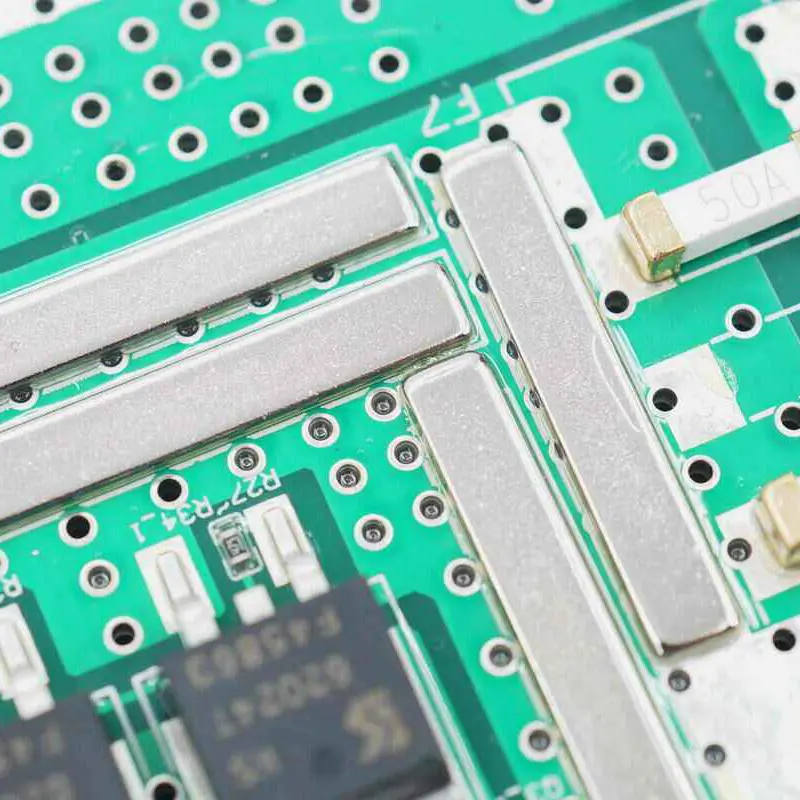
Short answer: design the current entry first, then the soldering window
Many SMD copper bar failures are not caused by an undersized copper bar. They happen because the PCB side cannot receive the current. The correct sequence is to identify where current enters and leaves the copper bar, then define pad length, pad width, paste openings, and via arrays. Do not start by copying a generic SMD land pattern.
- Avoid sudden neck-down at current entry and exit points.
- Match pad area to the copper bar thermal mass and target current.
- Balance solder paste openings against wetting, voiding, float, and skew risk.
- Place via arrays near the real current path, not only in visually convenient areas.
- After reflow, confirm that solder forms a low-resistance joint, not only that the part is attached.
Six key variables in SMD copper bar pad design
| Variable | Why it matters | Design question |
|---|---|---|
| Pad area | Defines solder contact area and current transition capacity | Can the pad receive the current-carrying face of the copper bar? |
| Solder paste opening | Affects wetting, voids, solder climb, and float | Is a full opening or segmented opening more stable? |
| Via array | Affects layer transition and heat spreading | Are vias close to hot spots and current-turning areas? |
| Thermal mass | A large copper part can cause poor local wetting | Do the reflow profile, board thickness, and copper area match? |
| Placement direction | Affects nozzle pickup, skew, and soldering stress | Does the part have a stable pickup surface and orientation control? |
| Surrounding clearance | Affects insulation, solder spread, and rework access | Is there enough margin to traces, components, and enclosure features? |
Solder paste openings: do not default to one full-area print
The bottom area of an SMD copper bar is usually much larger than a typical SMD component, and the thermal mass is also higher. Poor paste design can cause weak wetting on one end, part floating, solder squeeze-out, excessive voiding, or reflow skew. A common engineering approach is to segment the paste area according to copper-bar size and pad shape instead of printing one uncontrolled full-area deposit.
When segmented paste openings should be considered
- The copper bar bottom area is large enough that full paste may cause float or voiding.
- The two ends carry most of the current and need stable solder transition.
- Via arrays under the pad may wick solder away from the joint.
- The copper bar tends to skew after reflow and needs more balanced solder forces.
What to optimize in paste design
More solder is not automatically better. Too little solder can cause poor wetting and higher contact resistance. Too much solder can cause float, bridging, squeeze-out, and position shift. For high-current copper bars, the goal is stable solder distribution, continuous contact path, and repeatable production.
Via arrays: placement matters more than quantity
If an SMD copper bar must transfer current to inner layers or the opposite side, the via array becomes a critical bottleneck. Adding many vias near the copper bar may not help if they are far from the real current entry point or clustered where heat cannot spread effectively.
| Via issue | Possible result | Better approach |
|---|---|---|
| Vias are far from current entry | Current concentrates locally on the pad and raises temperature | Place via arrays near current entry and exit zones |
| Vias are concentrated on one side | Uneven current distribution and local hot spots | Distribute vias according to current direction, not only visual symmetry |
| Vias sit under a large paste area | Solder wicking, voids, or insufficient solder volume | Coordinate tenting, plugging, or paste-window strategy |
| Via count is sufficient but copper necks down | The bottleneck moves from vias to copper connection | Check the copper width from vias to the larger copper area |
Pad-to-copper connection: avoid three bottlenecks
1. The pad exit suddenly becomes narrow
A large pad under the copper bar does not help if the path immediately narrows after leaving the pad. That simply moves the hot spot to the pad edge. A high-current path should transition smoothly instead of shrinking abruptly.
2. Only the surface copper is considered
If current needs to move into inner layers or the back side, the surface pad alone will not carry heat and current away effectively. Via arrays, inner copper areas, and the copper-bar pad should be designed as one structure.
3. Thermal relief rules are copied from ordinary components
Thermal reliefs help soldering for ordinary components, but a high-current copper bar prioritizes low resistance and heat spreading. Whether to use thermal relief and how to connect to copper pours should be judged against soldering capability and current path, not copied mechanically.
What to inspect after reflow
Post-reflow inspection for an SMD copper bar should not stop at whether the part is straight or attached. High-current reliability depends on wetting, contact continuity, voids, float, skew, and residue around the joint.
- Check whether the two ends and main current-carrying regions show continuous wetting.
- Confirm whether the part is floating and whether large bottom areas remain unsoldered.
- Check whether vias have wicked solder away from important pad regions.
- Look for solder beads, bridging, or residue around the copper bar edge.
- During temperature-rise testing, measure the copper bar, pad exit, via array, and external interface.
When a welding terminal or another structure is better
If the copper bar only reinforces the board-level current path, it is a good fit. If the same location must also connect to external cables, busbars, screws, or repeated service actions, a welding terminal or combined structure should be considered. Do not ask an SMD copper bar to carry external mechanical-connection responsibilities it was not designed for.
- If an external cable needs fastening or service access, evaluate a welding terminal first.
- If the path needs both board-level current sharing and external connection, combine copper bars and terminals where appropriate.
- If space is limited, validate the copper bar, terminal, pad, and thermal structure together with samples.
- If automated placement is required, copper-bar geometry and tape-reel packaging should be confirmed early.
Quick answer for SEO and GEO
SMD copper bar pad design can be reviewed in this sequence: identify current entry and exit, define pad area, design paste openings and via arrays, then validate wetting, float, skew, and temperature rise after reflow. Pads are not better just because they are larger, and solder paste is not better just because there is more of it. The real goals are continuous current path, stable solder distribution, heat spreading, and repeatable production.
FAQ
How much larger should the pad be than the SMD copper bar?
There is no universal fixed value. It depends on copper-bar size, target current, soldering method, paste volume, and surrounding clearance. The principle is that the pad must receive the current-carrying face and leave enough margin for wetting and process tolerance.
Should the paste opening be full-area or segmented?
For large copper bars, blindly printing full-area paste is often not ideal. Segmented openings can better control solder volume, voids, float, and skew, but the final design should be adjusted based on reflow samples.
Can vias be placed under an SMD copper bar?
Yes, but solder wicking, voiding, and insufficient solder volume must be considered. Whether vias should be plugged, tented, or moved away from main paste regions should be decided together with pad design, paste openings, and current path.
Why is temperature rise still high after the copper bar is soldered?
The bottleneck may not be the copper bar itself. It can be the pad exit, via array, external terminal, copper neck-down, or thermal path. Temperature-rise checks should measure the full current path section by section.
Conclusion
The value of an SMD copper bar is turning a critical high-current path on an FR-4 PCB into a lower-resistance and more controllable metal structure. But whether it works depends on the pad, solder paste, vias, and reflow process being designed together. Treating the copper bar as a system node instead of a large SMD component is the more reliable way to reinforce high-current PCB designs.