


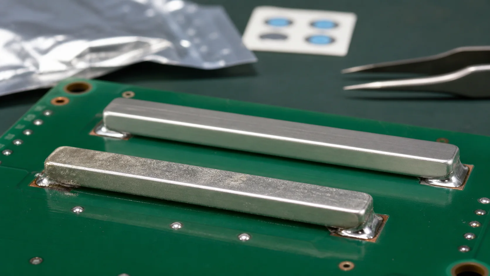
Quick answer: When an SMD busbar shows poor wetting, solder beading or exposed areas after storage, do not immediately raise the reflow peak temperature. First separate plating oxidation, surface contamination, packaging failure, insufficient flux activity and reflow-window drift. Compare a fresh control lot, the stored lot and a validated cleaned group in a solderability retest. Baking may remove moisture from some materials or packaging systems, but it does not reverse an existing metal oxide film. Production disposition should rely on sample testing, solder-joint cross sections, pull/shear strength and powered temperature rise.
Questions answered on this page
- Why can an SMD busbar solder well on arrival but show poor solderability after several months?
- How can oxidation or contamination on tin-, nickel- or silver-plated surfaces be screened?
- Do sealed packaging, desiccant and humidity indicators matter for metal parts?
- Can SMD busbars beyond the supplier shelf life be loaded directly into production?
- When do baking, cleaning, stronger flux or higher temperature help, and when do they hide the root cause?
- How should a stored lot be retested for solderability, joint strength and temperature rise?
Engineering summary
- Poor solderability after storage does not automatically mean the copper core has failed; check the solderable surface, packaging and process match first.
- A surface can still look bright while carrying a thin oxide, organic film or sulfur-related contamination. Visual inspection cannot replace solderability testing.
- Baking mainly removes moisture from compatible materials or packaging systems; it is not a universal repair for oxidized plating.
- Raising reflow temperature may temporarily improve wetting while increasing PCB, paste or plating risk.
- Use of an expired lot should be based on lot sampling, solderability, post-reflow appearance, cross section, strength and electrical performance.
Application context
Engineering issues such as “SMD busbar poor solderability after storage”, “tin-plated copper busbar oxidation”, “solder beading on PCB busbar” or “busbar shelf life” usually appear during inventory reuse, line changeover, volume reflow or customer failure analysis. Adjusting only solder paste or oven settings can allow the same root cause to return with another lot.
Hongchuan Precision Hardware supplies SMD busbars, PCB welding terminals, SMT nuts and copper-aluminum connectors for high-current PCB hardware applications. This guide is intended for purchasing, warehouse, incoming inspection, SMT, process, quality and hardware teams.
Separate five common symptoms
| Symptom | Possible cause | First check |
|---|---|---|
| Solder beads or recedes | Oxide film, oil or low-surface-energy contamination | Lot solderability, cleaned control and surface analysis |
| Only local areas reject solder | Uneven plating, fingerprints or packaging abrasion | Defect distribution, XRF/microscope and package contact points |
| Whole lot wets more slowly | Storage aging, packaging failure or paste activity change | Storage time, opening record, paste and profile comparison |
| One end wets and the other remains exposed | Thermal imbalance, pad temperature, placement or surface difference | Profile points, pad design and component orientation |
| Surface yellows or darkens after reflow | Plating oxidation, flux residue or excessive time/temperature | Pre/post reflow comparison, profile, residue and plating |
Why storage changes solderability
SMD busbar solderability is controlled by the outermost surface that contacts molten solder. Even with a highly conductive copper core, solder must wet the tin, nickel, silver or other final finish. Oxygen, moisture, sulfur compounds, packaging volatiles, fingerprints, dust and abrasion can change that outer layer during storage.
Higher temperature and humidity, poor sealing and long opened-pack exposure generally accelerate surface change. Each finish has different sensitivities: tin surfaces require control of oxidation, contamination and finish condition; silver surfaces can discolor through sulfur exposure; nickel is often a barrier layer, but direct solderability depends on the complete finish design. For finish selection, see tin, nickel and silver plating for SMD busbars.
Can appearance confirm oxidation?
Appearance is a screening tool, not a release criterion. Yellowing, gray haze, spots, fingerprints or local loss of gloss justify isolation, but a bright surface can still carry a very thin oxide or organic film that slows wetting.
Photograph a fresh lot, stored lot and failed parts under the same lighting, angle and magnification. If defects cluster at carrier-pocket contact points, pouch folds or manual handling areas, review packaging abrasion, material compatibility and glove practice.
Packaging, desiccant and opened-pack control
| Control | Purpose | Typical loss of control |
|---|---|---|
| Sealed barrier package | Reduce moisture and contaminant entry | Incomplete seal, pinhole or repeated opening |
| Desiccant | Absorb residual package moisture | Unknown quantity or reused after exposure |
| Humidity indicator | Support evaluation of moisture exposure | Checked too late, expired card or missing record |
| Carrier and cover tape | Protect finish, orientation and pick surface | Pocket abrasion, dust or cover-tape adhesive contamination |
| Opened-pack label | Record opening time, lot and remaining quantity | Date only, with no environment or reseal condition |
| FIFO | Reduce extended storage and mixed lots | Loss of original lot and shelf-life data after splitting |
Metal parts still depend on packaging for finish protection and SMT handling. For carrier dimensions, nozzle pickup, orientation and abrasion control, see tape-and-reel packaging for SMD copper busbars.
Does shelf-life expiration require automatic scrap?
Shelf life is the supplier's quality-commitment boundary under specified package, transport and storage conditions. It should not be judged only by the calendar, but an expired lot should not be loaded automatically. Isolate the lot, review package integrity, storage temperature and humidity, opening history and appearance, then run the required solderability retest.
A passed retest does not create unlimited extension. Define a new controlled use window, approved projects, released quantity and retained samples. If packaging is damaged, lot identity is lost, surface defects cluster or test variation is large, involve the supplier instead of consuming inventory through line trials.
What baking can and cannot solve
- Potentially useful: moisture in a compatible packaging, carrier, PCB or related material system, with a validated baking condition.
- Usually not repaired: metal-finish oxidation, sulfur tarnish, oil contamination or pore corrosion in the plating.
- New risks: carrier deformation, cover-tape change, further surface aging or lot mix-up after excessive heat or time.
Do not make “bake and load” the default response. Identify which material absorbed moisture and the failure mechanism, then define temperature, time, packaging compatibility and retest requirements with material, packaging, SMT and quality owners.
Can cleaning or stronger flux recover the lot?
A compatible solvent cleaning process may remove some oil or organic contamination, but it does not guarantee removal of a dense oxide film. Uncontrolled wiping can damage plating or spread contamination. Stronger flux activity may improve wetting, but it also changes residue, cleaning, corrosion and process windows.
If a validated cleaned group improves clearly while the as-stored group fails, identify the contamination source and confirm a repeatable production cleaning process. If only aggressive flux passes, reassess post-solder residue, ionic contamination and environmental reliability instead of accepting the lot because the joint looks bright.
How to structure a solderability retest
- Fresh control. Use a recent accepted lot to establish normal wetting time, coverage and joint appearance.
- As-stored group. Do not clean or bake; preserve the actual lot condition.
- Cleaned control. Use a confirmed compatible cleaning process to identify removable contamination.
- Process-boundary group. Compare approved low and high limits for paste and reflow without exceeding material limits.
- Post-reflow validation. Check wetting area, voiding, exposed finish, movement and pull/shear strength.
- Electrical group. Measure voltage drop, contact resistance and temperature rise at realistic current and cooling.
Use production-equivalent pad geometry, paste, stencil, placement orientation and reflow profile. A solder-dip screen can help evaluate the surface, but it does not fully replace an actual PCB reflow build.
Data to record during reflow
| Data | Purpose | Key interpretation |
|---|---|---|
| Busbar body and both pad temperatures | Confirm the high-thermal-mass part reaches the wetting window | End-to-end difference, time above liquidus and peak |
| Solder-paste lot and conditioning | Separate paste activity and working-life effects | Lot, open time, mixing and printing condition |
| Stencil and SPI data | Confirm paste volume and symmetry | Insufficient paste, offset, blocked aperture and variation |
| Placement coordinates and force | Confirm contact between busbar and paste deposits | Offset, paste collapse, nozzle contamination and part warp |
| AOI, X-ray and cross section | Evaluate hidden joint condition | Non-wetting, voids, cracks and effective bonded area |
If stored parts show non-wetting, voids or uneven solder, use the SMD busbar reflow void and poor-wetting troubleshooting guide to review stencil, wetting, X-ray and temperature rise.
Why strength and temperature rise still matter
A joint that barely accepts solder is not necessarily reliable. Reduced wetting area lowers mechanical strength and forces current through a smaller real bonded area, which can increase local current density and heating. Correlate pull/shear strength, effective bonded area in cross section, segmented voltage drop and powered temperature rise on the same sample groups.
If the hot spot appears at the pad exit rather than the joint, continue with copper neck and via-array analysis using the SMD busbar pad-exit temperature-rise guide.
Stored-lot disposition table
| Result | Suggested status | Next step |
|---|---|---|
| Package intact, within shelf life and equivalent to fresh control | Normal use | Retain records and maintain FIFO |
| Expired, package intact and stable retest pass | Controlled release | Limit time window, project and quantity; retain samples |
| Passes after cleaning but fails as stored | Do not load directly | Identify contamination and validate production cleaning |
| Large wetting variation or local exposed finish | Quarantine | Add plating/surface analysis and supplier review |
| Strength or temperature rise fails | Reject release | Do not consume the lot through cosmetic rework |
Production and warehouse controls
- Retain part number, finish, lot, production date, package date and recommended use period on incoming labels.
- Record warehouse conditions, package integrity, opening time, reseal time and remaining quantity.
- Keep original lot traceability after splitting and prevent mixing dates or finish lots.
- Screen long-stored inventory before loading; do not use the first production board as the only test sample.
- Freeze remaining material and corresponding PCB/paste data when an abnormality appears.
- Define retest method, sample size, release authority and extension window in the material-control process.
Common mistakes
- Declaring oxidation only because a surface looks dark, or releasing it only because it looks bright.
- Treating baking as the standard repair for every stored-lot solderability problem.
- Forcing wetting through higher peak temperature or aggressive flux without validating residue and reliability.
- Checking only joint appearance without cross section, strength, contact resistance and temperature-rise correlation.
- Loading expired inventory for a line trial and mixing an abnormal lot with normal production.
Purchasing, warehouse and process checklist
- Busbar material, finish stack, plating-thickness requirement and definition of the solderable surface.
- Production date, package date, recommended use period, packaging method and storage condition.
- Barrier pouch, desiccant, humidity indicator, carrier, cover tape and opened-pack/reseal record.
- Visual reference, solderability method, reflow test board, cross section, strength and temperature-rise criteria.
- Expired-lot quarantine, retest, controlled release, extension window and supplier communication.
FAQ
Does a dark SMD busbar surface always mean oxidation?
No. It may be sulfur tarnish, flux residue, packaging abrasion, oil or normal finish color variation. Use lot distribution, cleaned controls and solderability testing.
Can stored busbars be loaded immediately after baking?
Not by default. Baking does not repair metal oxidation and may affect carrier or surface condition. Identify the moisture source and complete solderability and real-reflow retesting first.
Can an expired lot be used if the sealed package is intact?
It can enter a controlled retest process, but package appearance alone is not enough. Review records and run lot-based solderability, joint and necessary electrical validation.
What can Hongchuan support?
Hongchuan can support SMD busbar part selection, material and plating, tape-and-reel packaging, samples and initial pad or reflow recommendations. The high-current PCB hardware selection guide can help coordinate busbars with welding terminals and SMT nuts.