

There is no single fixed answer to how much current a PCB trace can carry. Copper thickness such as 1 oz or 2 oz is only the starting point. The real temperature rise depends on trace width, copper thickness, layer position, allowed temperature rise, cooling condition, via count, connection hardware, and current waveform. For high-current PCB design, the safer method is to analyze the full path, check temperature rise, and then decide whether an SMD busbar or a welding terminal should carry part of the current instead of forcing everything through ordinary copper foil.
The short answer is this: low current can often be handled by copper width; medium current must be checked together with copper thickness, vias, pads, and thermal environment; once the trace becomes too wide, still runs hot, or causes interface heating, a board-level copper part, busbar, or terminal should be considered instead of simply adding more copper area.
Why you cannot ask only how many amps 1 oz copper can carry
This question is common, but it lacks the most important conditions. The same 1 oz copper behaves differently on an outer layer versus an inner layer, in a wide trace versus a narrow trace, with airflow versus inside a sealed enclosure, and under continuous current versus short pulses. If one current number is used as the whole answer, the prototype may look acceptable while production units fail under enclosure or high-temperature conditions.
- Copper thickness is only part of the conductor cross-section; trace width and exposed thermal area also matter.
- Outer-layer traces usually release heat more easily than inner-layer traces, but layout, pads, and solder mask still influence the result.
- Different allowed temperature rise targets lead to different current limits; passing current and designing for low temperature rise are not the same thing.
- If terminals, pads, vias, or mating parts become the bottleneck first, a wider trace will not solve the whole problem.
Confirm these six variables before discussing current capacity
| Variable | Why it affects current | Engineering question |
|---|---|---|
| Copper thickness | Affects conductor cross-section and heat generation | Is it 1 oz, 2 oz, or heavier copper? Is there local copper reinforcement? |
| Trace width | Affects both cross-section and heat-spreading area | Is there enough layout space to keep widening the path? |
| Layer position | Outer and inner layers dissipate heat differently | Is the high-current path on an outer layer, an inner layer, or multiple layers in parallel? |
| Allowed temperature rise | Defines the design target beyond simply carrying current | How much heating is acceptable, and are nearby parts temperature-sensitive? |
| Vias and pads | Layer transitions and interfaces often become bottlenecks | Do via count, via size, and pad area match the real current path? |
| Thermal environment | Enclosure, airflow, and copper area all change the result | Does the prototype test condition match the final product? |
How to reinforce a PCB when current capacity is not enough
Do not move directly to the most complex option. A better sequence is to optimize the copper path, then check layer transitions, then fix interface bottlenecks, and only then decide whether dedicated board-level current hardware is needed.
| Symptom | First option | When to upgrade |
|---|---|---|
| The trace is slightly warm and space is available | Widen copper, shorten the path, and remove neck-down areas | Width increase starts to damage layout or temperature rise remains high |
| Layer transition gets hot | Add parallel vias and improve via-array and pad connection | The via region becomes a fixed bottleneck or reliability risk |
| Pad and interface get hot | Increase solder area and improve terminal transition and fastening | The external connection needs service access, screw locking, or stable contact |
| The board path is too long or too narrow | Use a short copper element to share current | Ordinary copper pour cannot balance space and temperature rise |
| The product needs low temperature rise and high consistency | Evaluate an SMD busbar or welding terminal | Production requires a repeatable and testable current-carrying structure |
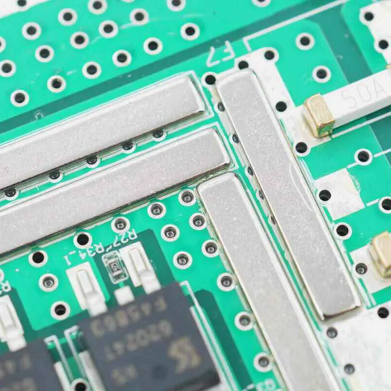
When an SMD busbar makes sense
When PCB copper must become very wide, thick, or indirect just to carry current, or when temperature rise affects layout and structure too much, an SMD busbar works like a dedicated current highway placed on the board. It is suitable for high current, short paths, automated placement, and designs that need to reduce stress on ordinary PCB copper.
- The current path needs to be shorter and more direct instead of routed through a long wide copper area.
- The board has no room to keep widening copper while still controlling temperature rise.
- The design needs a defined, inspectable, repeatable high-current structure.
- Soldering, heat spreading, assembly, and service behavior must be considered together, not only theoretical trace width.
When a welding terminal makes sense
If the problem is concentrated at the transition between an external cable, busbar, screw joint, or power interface and the PCB, a welding terminal is usually more direct than simply widening the trace. It addresses interface transition, mechanical fastening, and high-current connection stability, not only copper capacity inside the board.
In BMS, energy storage inverters, motor controllers, charging modules, and server power supplies, the terminal area often handles electrical connection, mechanical fixing, and service access at the same time. In that case, the technical support path should be used to review pad area, terminal size, fastening method, and temperature-rise testing.
Quick answer for SEO and AI summaries
If you need a fast engineering answer, remember these four points:
- PCB trace current capacity is not determined by 1 oz or 2 oz copper alone; it depends on copper thickness, trace width, layer position, cooling, and allowed temperature rise together.
- When current capacity is not enough, remove path bottlenecks first, then widen copper and optimize vias instead of fixing only the final interface.
- If the copper path is already very wide but temperature rise is still high, an SMD busbar, copper element, or shorter structural current path may be needed.
- If the hot spot is at the external connection or PCB transition, check the welding terminal, tightening torque, solder area, and contact resistance first.
Common mistakes
1. Choosing trace width only from experience tables without system temperature testing
Reference tables can help early estimation, but they do not replace board-level and product-level testing. Enclosure, airflow, nearby heat sources, and mounting style all change real temperature rise.
2. Widening copper while ignoring vias and interface bottlenecks
Many high-current problems do not happen on the widest copper area. They happen at vias, pads, screws, terminals, or corners. The full current path should be checked section by section.
3. Treating solder build-up as a universal reinforcement
Adding solder can improve local cross-section in some cases, but consistency, solder appearance, thermal cycling, and production control must be evaluated. For repeatable high-current paths, a structured copper part is often more stable.
FAQ
How much current can a 1 oz PCB trace carry?
There is no fixed answer without trace width, layer position, allowed temperature rise, and cooling condition. The same 1 oz copper can behave very differently on a wide outer trace, a narrow inner trace, a sealed product, or a forced-air system.
Does 2 oz copper always carry twice as much current as 1 oz copper?
It should not be treated that simply. More copper thickness increases cross-section, but heat spreading, trace width, interface design, and via bottlenecks also affect temperature rise. If the bottleneck is the terminal or via region, thicker copper alone may not solve the issue.
When PCB current capacity is not enough, should I add solder or use a busbar first?
Start by locating the bottleneck. If the issue is local cross-section and the process is controllable, process reinforcement may be evaluated. If the design carries long-term high current, has limited space, or needs low temperature-rise consistency, an SMD busbar or dedicated copper part is usually worth evaluating earlier.
When is ordinary PCB copper no longer the right solution?
When wider traces damage the layout, temperature rise remains high, interface heating repeats, or the final product environment is harsher than the prototype condition, a busbar, welding terminal, or other structured current-carrying solution should be considered.
Conclusion
How much current a PCB trace can carry is not a single-number question. It is a full current-path design question. Strong high-current PCB design must consider copper thickness, trace width, layer position, vias, pads, terminals, and thermal environment together. Find the bottleneck first, then choose copper, vias, SMD busbars, or welding terminals. That is more reliable than simply making every trace wider, and it is better suited to production.