

PCB Copper Strip Selection Guide: 5 Key Parameters for Engineers
1. Why is Copper Strip Selection Critical?
In BMS, solar inverters, and energy storage systems, high-current PCB conduction is a core challenge. Improper copper strip selection can lead to:
- Excessive temperature rise: Heat generated during operation affects device lifespan
- Excessive voltage drop: Power loss increases, system efficiency decreases
- Poor solder joint reliability: Thermal expansion mismatch causes cold solder joints
- Space waste: Oversized parts increase PCB area costs
This guide provides a systematic approach to copper strip selection from an engineer's perspective.
2. Key Selection Parameters
2.1 Material Selection
| Material | Conductivity | Characteristics | Applications |
|---|---|---|---|
| Pure Copper (T2) | 100% IACS | Best conductivity, soft and easy to process | High-current, high-reliability applications |
| Brass (H62) | 28% IACS | High hardness, good wear resistance | Applications requiring mechanical strength |
| Tin-Plated Copper | 85-90% IACS | Oxidation resistance, easy soldering | Long-term storage or multiple soldering |
Recommendation: For new energy PCB applications, pure copper (T2) is preferred with optimal conductivity and best cost-performance.
View Hongchuan's copper strip products - all made from premium pure copper.
2.2 Thickness Specifications
Copper thickness is key to current-carrying capacity. Industry standard uses oz (ounces):
| Copper Weight | Thickness (mm) | Typical Applications |
|---|---|---|
| 1oz | 0.035 | Low-power consumer electronics |
| 2oz | 0.070 | General industrial control |
| 3oz | 0.105 | Energy storage BMS |
| 4oz | 0.140 | Solar inverters |
| 6oz+ | 0.210+ | High-power charging stations |
Rule of thumb: Increase copper cross-section by ~0.05mm² for each additional Ampere
2.3 Width Design
Width directly affects temperature rise and voltage drop. Consider:
- Current capacity: Wider = higher current
- PCB layout space: Coordinate with surrounding components
- Impedance matching: Consider skin effect for high-frequency signals
Quick Reference (2oz copper, 25℃ ambient, 10℃ temp rise):
| Current (A) | Minimum Width (mm) |
|---|---|
| 1 | 0.5 |
| 3 | 1.0 |
| 5 | 1.5 |
| 10 | 3.0 |
2.4 Surface Treatment
| Treatment | Characteristics | Cost |
|---|---|---|
| Bare Copper | Best conductivity | Low |
| Tin Plating | Oxidation resistance, good solderability | Medium |
| Nickel Plating | Corrosion resistance, wear resistance | Medium-High |
| Immersion Silver | High reliability (military grade) | High |
| ENIG | Gold appearance, long-term stability | High |
Recommendation: Tin plating for general industrial applications; Immersion Silver or ENIG for high-reliability scenarios.
2.5 Application Matching
Solar Inverters
- Current range: 15-50A
- Recommended: 3-4oz, width 8-20mm
- Key requirements: Low impedance, high-temperature resistance
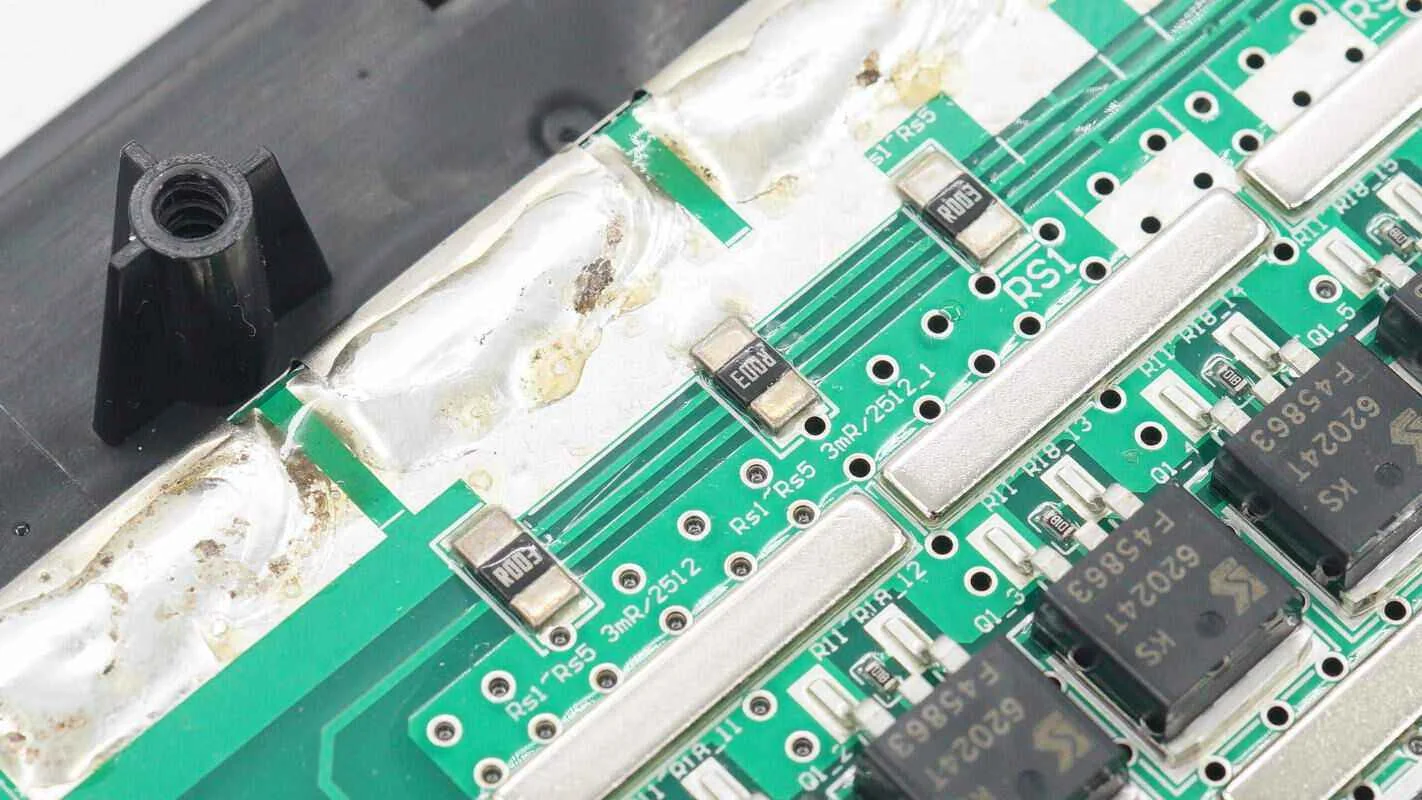
Energy Storage BMS
- Current range: 5-30A
- Recommended: 2-3oz, width 5-15mm
- Key requirements: Multi-channel parallel, consistency
Charging Stations
- Current range: 30-100A
- Recommended: 6oz+, width 25-50mm
- Key requirements: High current capacity, thermal design
3. Step-by-Step Selection Process
Step 1: Determine Operating Current
Calculate based on system power:I = P / U
Example: 1000W @ 48V system → I ≈ 21A
Step 2: Calculate Copper Cross-Section
Using the formula:S = I × 0.05 (mm²/A)
21A × 0.05 = 1.05mm²
Step 3: Select Thickness and Width
Assuming 2oz (0.07mm thickness):Width = 1.05 / 0.07 ≈ 15mm
Step 4: Verify Temperature Rise
Use current capacity tables or simulation tools to verify temperature rise meets design requirements (typically ≤30℃).
Step 5: Confirm Manufacturing Process
- Soldering method: Reflow / Wave / Hand soldering
- Tolerance: ±0.1mm (precision) or ±0.2mm (general)
- Surface treatment: Plating thickness, color requirements
4. Common Selection Mistakes
❌ Mistake 1: Thickness only, ignore width
Increasing copper thickness costs significantly more than increasing width. Prioritize width over thickness.
❌ Mistake 2: Ignoring ambient temperature
Current ratings are based on 25℃ ambient. Derate for high temperatures:
- 50℃ environment → derate 20%
- 70℃ environment → derate 40%
❌ Mistake 3: Conductivity only, no thermal consideration
Current capacity is closely related to thermal conditions. Natural convection, forced air, and heat sinks all affect actual current capacity.
❌ Mistake 4: Ignoring PCB copper thickness matching
The PCB pad copper thickness at both ends of the copper strip must match, otherwise a "thermal bridge" effect occurs.
5. Hongchuan Precision Advantages
- ✅ 6000+ Standard Products: Same-day shipping for common specifications
- ✅ Customization Services: Non-standard sizes, rapid prototyping
- ✅ Full Parameter Testing: Material, dimension, electrical performance - 100% inspected
- ✅ Technical Support: Current capacity calculation and simulation advice
Hongchuan Precision, located in Dongguan Chang'an Town, specializes in new energy PCB high-current hardware manufacturing, including copper strips, SMD nuts, PCB welding terminals and more.
Contact Us
Phone: +86-18938685515
Address: No.319, Yixiang Long Road, Jinsha Community, Chang'an Town, Dongguan, Guangdong, China
Website: https://www.hc-sp.com/en/