


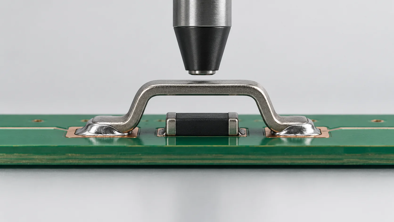
Direct answer Measure post-reflow jumper clearance as the minimum distance between the bridge underside and the highest obstacle below it. Catalog height, span and total length describe different dimensions. Request the height definition, tolerances and datums, then inspect the soldered assembly rather than treating a catalog figure as a board-level guarantee.
Separate A, B and height
Hongchuan's catalog lists BTC-SJE182BTR with span A of 10.70 mm and total length B of 14.10 mm. Its 1.8 mm catalog height needs confirmation against the model drawing and soldered condition. A and B are not interchangeable, and B alone does not establish usable space below the bridge. Confirm substrate and plating separately by model.
| Dimension | What to establish |
|---|---|
| Span A | Functional end positions and drawing definition |
| Total length B | Outline and placement keep-out |
| Bridge underside height | Reference surface and tolerance |
| Minimum assembled gap | Shortest distance to the actual obstacle |
A hypothetical tolerance envelope
Using the same local PCB datum and considering vertical separation only, gminimum = hbridge,minimum − hobstacle,maximum. Assume an assembled underside height of 1.80 ± 0.10 mm and an obstacle height of 0.90 ± 0.15 mm. The worst-case gap is 0.65 mm. These are assumed tolerances, not BTC-SJ series specifications.
Real assemblies also involve bridge tilt, unequal solder seating, board warpage and obstacle tilt. Do not deduct an effect twice if it is already included in the assembled height envelope. Otherwise include it in the model or measure the worst location directly. Without validated statistical assumptions, do not replace a worst-case check with a root-sum-square calculation.
Measure after reflow
Use a validated optical method or suitable gauge to check both sides and the lowest point over the crossing region. Retain side views, datums, locations and the minimum reading. Resolution and measurement uncertainty should suit the agreed gap. Do not force a feeler gauge into the gap and deform either component.
Start with the surface mount PCB jumper model table and the guide to copper strips versus SMT jumpers.
Frequently asked question
Does a mechanical 0.65 mm gap prove insulation compliance?
No. Clearance and creepage between different-potential conductors need the applicable product standard, voltage and environmental conditions. IEC 60664-1, including its 2025 amendment, addresses insulation coordination. Catalog board height alone cannot demonstrate compliance.
Sources
- Hongchuan jumper catalog, A, B and reference height.
- Keystone surface mount PCB jumpers, intended structure.
- IEC 60664-1 consolidated edition official scope.
Sources checked on 8 October 2026. Calculations are hypothetical examples, not Hongchuan product test data. The cover is an AI-generated engineering illustration, not a product photograph or test record.