


Stencil area ratio (AR) is aperture opening area divided by aperture wall area. For a rectangular SMD busbar aperture, AR = L × W/[2t(L + W)], using identical units. Check each sub-aperture after segmentation; a large total opening area does not establish reliable release from every small opening.
Separate three geometric quantities
Indium's stencil design application note defines AR and lists ≥0.66 as industry guidance. Treat it as an initial screen, not a universal acceptance limit across pastes, apertures and stencils. Aspect ratio W/t is a different quantity.
| Quantity | Formula | Meaning |
|---|---|---|
| Rectangular AR | L × W/[2t(L + W)] | Opening area / four wall areas |
| Square AR | D/(4t) | D is side length |
| Circular AR | D/(4t) | D is diameter |
| Rectangular aspect ratio | W/t | Not AR |
| Nominal aperture volume | L × W × t | mm³, not measured deposit volume |
A thicker stencil changes both volume and AR
For a hypothetical 0.30 mm square aperture and 100 μm (0.10 mm) thickness, AR = 0.75 and nominal volume = 0.009 mm³. At 150 μm (0.15 mm), AR falls to 0.50 while nominal volume rises to 0.0135 mm³. A 50% nominal increase does not demonstrate a 50% increase on the board. These are geometry examples, not recommended Hongchuan aperture dimensions.
AIM's area-ratio research examines limitations of a single threshold across stencil thicknesses. Its proposed model is conditional, not a product guarantee. Document paste formulation, powder grade, wall treatment and release conditions.
Choose with a controlled print trial
Hold paste batch, board support and printing settings constant when comparing agreed stencil options. Calculate transfer efficiency as measured SPI deposit volume / nominal aperture volume × 100%. Preserve calibration and segmentation settings. Compare variation, missing deposits and bridging as well as averages. Separate continuous prints from the first print after a pause. Follow with reflow inspection for coverage, displacement and floating.
If AR is low, discuss geometry, thickness and paste with suppliers rather than extending apertures into required electrical spacing. A proposed step stencil also needs a review of squeegee travel, support and neighboring deposits.
Send the process drawing
Provide solder-contact geometry, pads, every aperture size, thickness, paste identification and SPI results with an SMD busbar enquiry. The busbar pad and via guide covers the broader assembly. This aperture calculation does not replace board-level validation.
FAQ
Does AR ≥0.66 remove the need for trials? No; geometry does not capture the entire printing process.
Can I calculate AR from summed segmented area alone? Check individual openings and their walls. Totals can hide poor release from narrow segments.
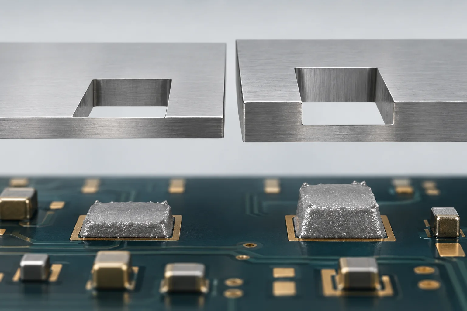
AI-generated stencil-process illustration. Dimensions and volumes are hypothetical, not product specifications, acceptance limits or production guarantees.