


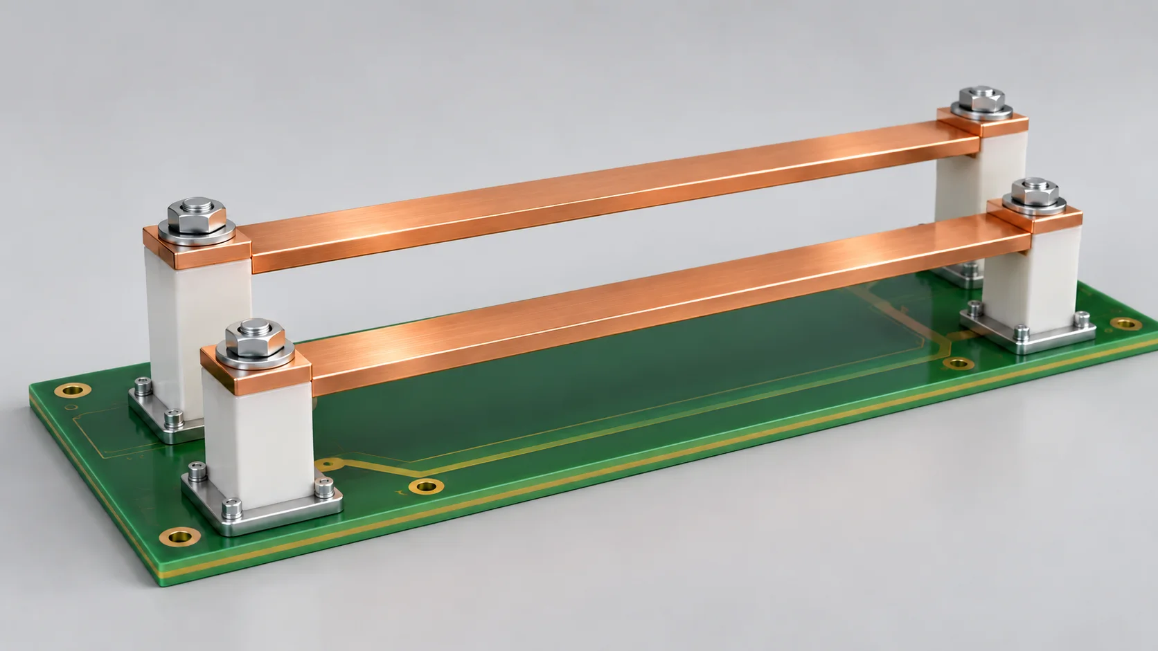
Direct answer A PCB busbar needs both thermal and mechanical short-circuit assessment. Magnetic force depends on the instantaneous current product. For equal currents, force scales with current squared. Obtain the fault waveform or peak, conductor spacing and support conditions; continuous operating current does not establish short-circuit withstand.
Separate the electrical inputs
| Input | Purpose | Units to record |
|---|---|---|
| Instantaneous peak and direction | Magnetic load and force direction | A, with time in s |
| Integral of current squared over time | Fault heating assessment | A²·s |
| Conductor separation and support span | Structural model | mm, converted consistently |
Battery impedance, DC-link capacitors and protective devices affect a DC PCB fault waveform. Ask the system designer for peak current, duration and current-limiting assumptions. IEC 60909-0:2026 covers 50 Hz or 60 Hz three-phase AC systems; it is not a direct DC board fault model.
A calculation for scale, not qualification
For sufficiently long, thin, parallel conductors in an approximately free-space field, force magnitude per length is F/L = μ₀|I₁I₂|/(2πd). Use current in A and centre spacing d in m. With μ₀ approximately 4π×10⁻⁷ H/m, the result is N/m. Parallel currents attract; opposite currents repel.
Assume opposite currents of 1000 A in each conductor and 10 mm centre spacing. The result is 20 N/m, or approximately 1 N over a uniformly loaded 50 mm length. At 2000 A, the same geometry gives approximately 4 N. These are idealised calculations, not a short-circuit rating for an SMD busbar.
What is missing before assessing the solder joints?
Wide rectangular sections, bends, neighbouring return paths and small gaps alter the field distribution. A soldered copper strip also does not automatically satisfy a freely supported beam model. Define material temper, section orientation, soldered regions, PCB constraints and support stiffness before selecting an analytical model, simulation or controlled test. Dividing the total force equally between two joints is not qualification evidence.
For a PCB busbar enquiry, provide the conductor layout, fault conditions, support locations and permitted deformation. The companion article explains peak current, RMS and I²t.
Frequently asked question
Will a thicker copper strip solve the problem?
It changes resistance and stiffness, but the supports, solder joints and PCB still need assessment. After a fault, isolate power under the equipment procedure and inspect permanent deformation, cracked joints, damaged supports and changed spacing before deciding whether the assembly can return to service.
Sources
- Copper for Busbars, Chapter 4.
- IEC 60909-0:2026 official scope.
Sources checked on 8 October 2026. Calculations are hypothetical examples, not Hongchuan product test data. The cover is an AI-generated engineering illustration, not a product photograph or test record.