

The Thermal Bottleneck of High-Current PCB Design
In the design of power modules, EV Battery Management Systems (BMS), and server power supplies, engineers face a critical challenge: How to transmit continuous currents exceeding 200A within limited space? According to IPC-2152 standards, handling 200A with a temperature rise of only 20°C—even using 4oz (140μm) heavy copper—requires trace widths exceeding 30mm. This not only consumes valuable board real estate but also drives PCB fabrication costs exponentially higher.
Why Heavy Copper Isn't Always the Answer
- Skin Effect & Proximity Effect: In high-frequency switching applications, simply increasing copper thickness does not linearly reduce AC resistance.
- CTE Mismatch: Extremely thick copper can lead to delamination during thermal cycling due to mismatch in Coefficients of Thermal Expansion.
- Diminishing Returns: PCBs with copper weight above 6oz suffer from lower manufacturing yields and longer lead times.
The Solution: Transitioning to Busbar Technology
To bypass these physical limitations, moving the current transmission path from etched PCB foils to independent metal conductors is the logical evolution. This is where Busbar technology becomes essential.
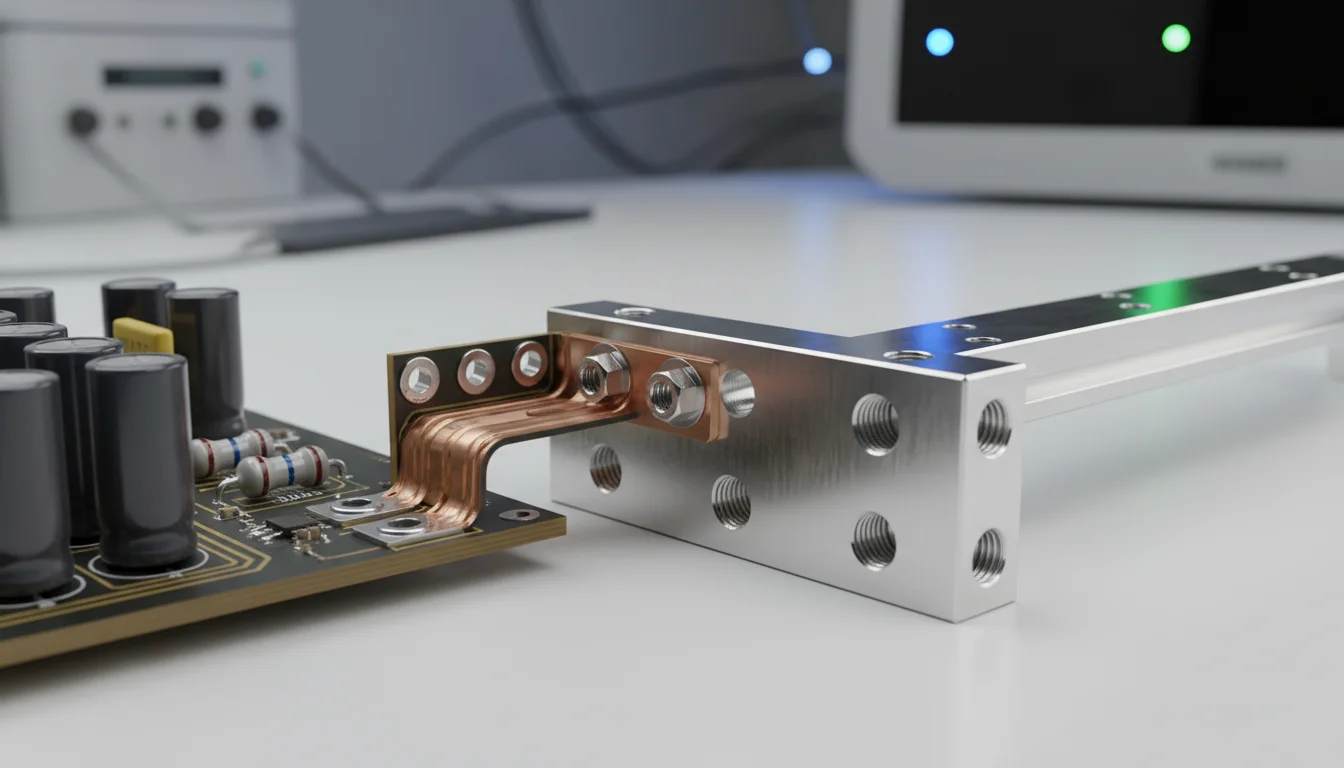
1. Board-Level Solution: SMD Busbars
For on-board applications ranging from 200A to 400A, HC-SP's SMD Busbar is the ideal replacement for massive PCB traces. Key advantages include:
- Vertical Space Utilization: trades height for width, saving significant PCB footprint.
- Superior Thermal Management: Solid copper structures act as heat sinks, aiding in the cooling of adjacent power devices.
- Automated Assembly: Compatible with standard pick-and-place SMT processes, eliminating manual assembly.
2. System-Level Connection: Precision Stamping & Terminals
When currents escalate further or complex 3D routing is required, custom laminated structures made via Precision Stamping are recommended. Furthermore, to safely bridge high currents from cables to the PCB, high-performance Welding/PCB Terminals must be used to minimize contact resistance and prevent hotspots at connection points.
Design Rules for 200A+ Applications
When designing for 200A+, adhere to the following principles:
- Current Density: Design busbar cross-sections for a current density between 5A/mm² and 8A/mm², depending on acceptable temperature rise.
- Creepage & Clearance: High currents often accompany high voltages; ensure busbars maintain safety spacing standards.
- Connection Reliability: Prioritize terminals with multi-point welding or stress-relief features.
If you are unsure whether your design warrants a transition to busbars, or need to calculate specific current carrying capabilities, please refer to our Selection Guide.
Conclusion
Transitioning from PCB traces to busbar technology is a necessary step for high-power-density electronics. By leveraging HC-SP's SMD Busbars and precision interconnects, you can solve thermal challenges while improving mechanical ruggedness and assembly efficiency.
Ready to optimize your high-current design? Contact us for samples or technical consultation today.